- 您现在的位置:买卖IC网 > PDF目录45206 > MC56F8245VLD (FREESCALE SEMICONDUCTOR INC) 16-BIT, FLASH, 60 MHz, MICROCONTROLLER, PQFP44 PDF资料下载
参数资料
| 型号: | MC56F8245VLD |
| 厂商: | FREESCALE SEMICONDUCTOR INC |
| 元件分类: | 微控制器/微处理器 |
| 英文描述: | 16-BIT, FLASH, 60 MHz, MICROCONTROLLER, PQFP44 |
| 封装: | 10 X 10 MM, 1.40 MM HEIGHT, 0.80 MM PITCH, ROHS COMPLIANT, PLASTIC, MS-026BCB, LQFP-44 |
| 文件页数: | 11/88页 |
| 文件大小: | 4050K |
| 代理商: | MC56F8245VLD |
第1页第2页第3页第4页第5页第6页第7页第8页第9页第10页当前第11页第12页第13页第14页第15页第16页第17页第18页第19页第20页第21页第22页第23页第24页第25页第26页第27页第28页第29页第30页第31页第32页第33页第34页第35页第36页第37页第38页第39页第40页第41页第42页第43页第44页第45页第46页第47页第48页第49页第50页第51页第52页第53页第54页第55页第56页第57页第58页第59页第60页第61页第62页第63页第64页第65页第66页第67页第68页第69页第70页第71页第72页第73页第74页第75页第76页第77页第78页第79页第80页第81页第82页第83页第84页第85页第86页第87页第88页
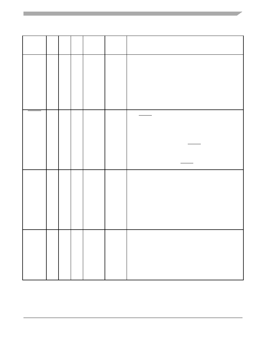
Signal/Connection Descriptions
MC56F825x/MC56F824x Digital Signal Controller, Rev. 3
Freescale Semiconductor
19
TMS
(GPIOD3)
43
47
63
input
Input/
Output
Input,
internal
pullup
enabled
Test Mode Select Input — This input pin is used to sequence the
JTAG TAP controller’s state machine. It is sampled on the rising
edge of TCK and has an on-chip pullup resistor.
Port D GPIO — This GPIO pin can be individually programmed as
an input or output pin.
After reset, the default state is TMS
Note: Always tie the TMS pin to VDD through a 2.2K resistor if need
to keep on-board debug capability. Otherwise directly tie to VDD
RESET
(GPIOD4)
222
Input
Input/
Open-drain
Output
Input,
internal
pullup
enabled
Reset — This input is a direct hardware reset on the processor.
When RESET is asserted low, the device is initialized and placed in
the reset state. A Schmitt-trigger input is used for noise immunity.
The internal reset signal is deasserted synchronous with the
internal clocks after a fixed number of internal clocks.
Port D GPIO — This GPIO pin can be individually programmed as
an input or open-drain output pin.If RESET functionality is disabled
in this mode and the chip can be reset only via POR, COP reset, or
software reset.
After reset, the default state is RESET.
GPIOA0
(ANA0&
CMPA_P2)
(CMPC_O)
8
9
13
Input/
Output
Input
Output
Input,
internal
pullup
enabled
Port A GPIO — This GPIO pin can be individually programmed as
an input or output pin.
ANA0 and CMPA_P2 — Analog input to channel 0 of ADCA and
positive input 2 of analog comparator A.
CMPC_O— Analog comparator C output
When used as an analog input, the signal goes to the ANA0 and
CMPA_P2.
After reset, the default state is GPIOA0.
GPIOA1
(ANA1&
CMPA_M0)
9
10
14
Input/
Output
Input
Input,
internal
pullup
enabled
Port A GPIO — This GPIO pin can be individually programmed as
an input or output pin.
ANA1 and CMPA_M0 — Analog input to channel 1of ADCA and
negative input 0 of analog comparator A.
When used as an analog input, the signal goes to the ANA1 and
CMPA_M0.
After reset, the default state is GPIOA1.
Table 5. MC56F825x/MC56F824x Signal and Package Information (continued)
Signal
Name
44
LQFP
48
LQFP
64
LQFP
Type
State
During
Reset
Signal Description
相关PDF资料 |
PDF描述 |
|---|---|
| MC56F8245MLD | 16-BIT, FLASH, 60 MHz, MICROCONTROLLER, PQFP44 |
| MC56F8322MFAE | 0-BIT, 120 MHz, OTHER DSP, PQFP48 |
| MC56F8322VFAE | 0-BIT, 120 MHz, OTHER DSP, PQFP48 |
| MC56F8347VPY60 | 16-BIT, 120 MHz, OTHER DSP, PQFP160 |
| MC56F8347MPY60 | 16-BIT, 120 MHz, OTHER DSP, PQFP160 |
相关代理商/技术参数 |
参数描述 |
|---|---|
| MC56F8246 | 制造商:FREESCALE 制造商全称:Freescale Semiconductor, Inc 功能描述:Digital Signal Controller Battery chargers and management |
| MC56F8246MLF | 功能描述:数字信号处理器和控制器 - DSP, DSC DSC 48 LQFP 48K FL RoHS:否 制造商:Microchip Technology 核心:dsPIC 数据总线宽度:16 bit 程序存储器大小:16 KB 数据 RAM 大小:2 KB 最大时钟频率:40 MHz 可编程输入/输出端数量:35 定时器数量:3 设备每秒兆指令数:50 MIPs 工作电源电压:3.3 V 最大工作温度:+ 85 C 封装 / 箱体:TQFP-44 安装风格:SMD/SMT |
| MC56F8246VLF | 功能描述:数字信号处理器和控制器 - DSP, DSC DSC 48 LQFP 48K FL RoHS:否 制造商:Microchip Technology 核心:dsPIC 数据总线宽度:16 bit 程序存储器大小:16 KB 数据 RAM 大小:2 KB 最大时钟频率:40 MHz 可编程输入/输出端数量:35 定时器数量:3 设备每秒兆指令数:50 MIPs 工作电源电压:3.3 V 最大工作温度:+ 85 C 封装 / 箱体:TQFP-44 安装风格:SMD/SMT |
| MC56F8247 | 制造商:FREESCALE 制造商全称:Freescale Semiconductor, Inc 功能描述:Digital Signal Controller Battery chargers and management |
| MC56F8247MLH | 功能描述:数字信号处理器和控制器 - DSP, DSC DSC 64 LQFP 48K FL RoHS:否 制造商:Microchip Technology 核心:dsPIC 数据总线宽度:16 bit 程序存储器大小:16 KB 数据 RAM 大小:2 KB 最大时钟频率:40 MHz 可编程输入/输出端数量:35 定时器数量:3 设备每秒兆指令数:50 MIPs 工作电源电压:3.3 V 最大工作温度:+ 85 C 封装 / 箱体:TQFP-44 安装风格:SMD/SMT |
发布紧急采购,3分钟左右您将得到回复。