- 您现在的位置:买卖IC网 > PDF目录10986 > MC56F8255VLD (Freescale Semiconductor)DSC 64K FLASH 60MHZ 44-LQFP PDF资料下载
参数资料
| 型号: | MC56F8255VLD |
| 厂商: | Freescale Semiconductor |
| 文件页数: | 28/88页 |
| 文件大小: | 0K |
| 描述: | DSC 64K FLASH 60MHZ 44-LQFP |
| 标准包装: | 160 |
| 系列: | 56F8xxx |
| 核心处理器: | 56800E |
| 芯体尺寸: | 16-位 |
| 速度: | 60MHz |
| 连通性: | CAN,I²C,LIN,SCI,SPI |
| 外围设备: | LVD,POR,PWM,WDT |
| 输入/输出数: | 35 |
| 程序存储器容量: | 64KB(32K x 16) |
| 程序存储器类型: | 闪存 |
| RAM 容量: | 4K x 16 |
| 电压 - 电源 (Vcc/Vdd): | 3 V ~ 3.6 V |
| 数据转换器: | A/D 8x12b,D/A 1x12b |
| 振荡器型: | 内部 |
| 工作温度: | -40°C ~ 105°C |
| 封装/外壳: | 44-LQFP |
| 包装: | 管件 |
第1页第2页第3页第4页第5页第6页第7页第8页第9页第10页第11页第12页第13页第14页第15页第16页第17页第18页第19页第20页第21页第22页第23页第24页第25页第26页第27页当前第28页第29页第30页第31页第32页第33页第34页第35页第36页第37页第38页第39页第40页第41页第42页第43页第44页第45页第46页第47页第48页第49页第50页第51页第52页第53页第54页第55页第56页第57页第58页第59页第60页第61页第62页第63页第64页第65页第66页第67页第68页第69页第70页第71页第72页第73页第74页第75页第76页第77页第78页第79页第80页第81页第82页第83页第84页第85页第86页第87页第88页
MC56F825x/MC56F824x Digital Signal Controller, Rev. 3
Memory Maps
Freescale Semiconductor
34
The 56F824x’s startup address is located at 0x00 2000. The reset value of VBA is reset to a value of 0x0020 that
corresponds to the address 0x00 2000.
By default, the chip reset address and COP reset address correspond to vector 0 and 1 of the interrupt vector table. In these
instances, the first two locations in the vector table must contain branch or JMP instructions. All other entries must contain JSR
instructions.
Table 48 on page 85 provides the MC56F825x/MC56F824x’s interrupt table contents and interrupt priority structure.
4.5
Peripheral Memory-Mapped Registers
The locations of on-chip peripheral registers are part of the data memory map on the 56800E series. These locations may be
accessed with the same addressing modes used for ordinary data memory. However, all peripheral registers should be read or
written using word accesses only.
Table 12 summarizes the base addresses for the set of peripherals on the MC56F825x/MC56F824x devices. Peripherals are
listed in order of the base address.
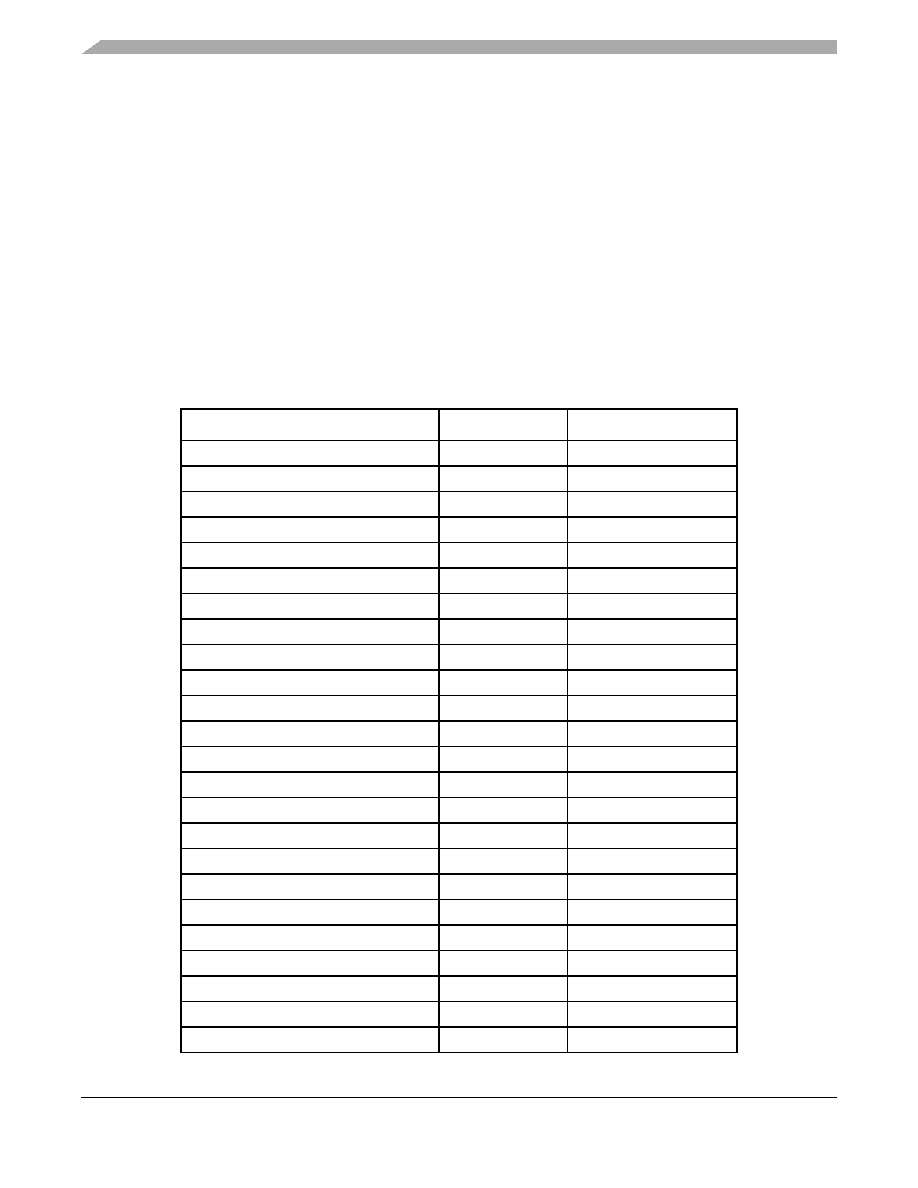
Table 12. Data Memory Peripheral Base Address Map Summary
Peripheral
Prefix
Base Address
Quad Timer A
TMRA
X:0x00 F000
Quad Timer B
TMRB
X:0x00 F040
Analog-to-Digital Converter
ADC
X:0x00 F080
Interrupt Controller
INTC
X:0x00 F0C0
System Integration Module
SIM
X:0x00 F0E0
Crossbar module
XBAR
X:0x00 F100
Computer Operating Properly module
COP
X:0x00 F110
On-Chip Clock Synthesis module
OCCS
X:0x00 F120
Power Supervisor
PS
X:0x00 F130
GPIO Port A
GPIOA
X:0x00 F140
GPIO Port B
GPIOB
X:0x00 F150
GPIO Port C
GPIOC
X:0x00 F160
GPIO Port D
GPIOD
X:0x00 F170
GPIO Port E
GPIOE
X:0x00 F180
GPIO Port F
GPIOF
X:0x00 F190
12-bit Digital-to-Analog Converter
DAC
X:0x00 F1A0
Analog Comparator A
CMPA
X:0x00 F1B0
Analog Comparator B
CMPB
X:0x00 F1C0
Analog Comparator C
CMPC
X:0x00 F1D0
Queued Serial Communication Interface 0
QSCI0
X:0x00 F1E0
Queued Serial Communication Interface 1
QSCI1
X:0x00 F1F0
Queued Serial Peripheral Interface
QSPI
X:0x00 F200
Inter-Integrated Circuit 0
I2C0
X:0x00 F210
Inter-Integrated Circuit 1
I2C1
X:0x00 F220
相关PDF资料 |
PDF描述 |
|---|---|
| VE-B6Z-IV-S | CONVERTER MOD DC/DC 2V 60W |
| MC9S08MM128CMB | IC MCU 8BIT 128K FLASH 81MAPBGA |
| VE-B6Y-IX-B1 | CONVERTER MOD DC/DC 3.3V 49.5W |
| DS21554LN | IC TXRX E1 1-CHIP 5V 100-LQFP |
| DS21552G | IC TXRX T1 1-CHIP 5V 100-BGA |
相关代理商/技术参数 |
参数描述 |
|---|---|
| MC56F8256 | 制造商:FREESCALE 制造商全称:Freescale Semiconductor, Inc 功能描述:Digital Signal Controller Battery chargers and management |
| MC56F8256MLF | 功能描述:数字信号处理器和控制器 - DSP, DSC DSC 48 LQFP 64K FL RoHS:否 制造商:Microchip Technology 核心:dsPIC 数据总线宽度:16 bit 程序存储器大小:16 KB 数据 RAM 大小:2 KB 最大时钟频率:40 MHz 可编程输入/输出端数量:35 定时器数量:3 设备每秒兆指令数:50 MIPs 工作电源电压:3.3 V 最大工作温度:+ 85 C 封装 / 箱体:TQFP-44 安装风格:SMD/SMT |
| MC56F8256VLF | 功能描述:数字信号处理器和控制器 - DSP, DSC DSC 48 LQFP 64K FL RoHS:否 制造商:Microchip Technology 核心:dsPIC 数据总线宽度:16 bit 程序存储器大小:16 KB 数据 RAM 大小:2 KB 最大时钟频率:40 MHz 可编程输入/输出端数量:35 定时器数量:3 设备每秒兆指令数:50 MIPs 工作电源电压:3.3 V 最大工作温度:+ 85 C 封装 / 箱体:TQFP-44 安装风格:SMD/SMT |
| MC56F8257 | 制造商:FREESCALE 制造商全称:Freescale Semiconductor, Inc 功能描述:Digital Signal Controller Battery chargers and management |
| MC56F8257MLH | 功能描述:数字信号处理器和控制器 - DSP, DSC DSC 64 LQFP 64K FL RoHS:否 制造商:Microchip Technology 核心:dsPIC 数据总线宽度:16 bit 程序存储器大小:16 KB 数据 RAM 大小:2 KB 最大时钟频率:40 MHz 可编程输入/输出端数量:35 定时器数量:3 设备每秒兆指令数:50 MIPs 工作电源电压:3.3 V 最大工作温度:+ 85 C 封装 / 箱体:TQFP-44 安装风格:SMD/SMT |
发布紧急采购,3分钟左右您将得到回复。