- 您现在的位置:买卖IC网 > PDF目录10985 > MC56F8256VLF (Freescale Semiconductor)DSC 64K FLASH 60MHZ 48-LQFP PDF资料下载
参数资料
| 型号: | MC56F8256VLF |
| 厂商: | Freescale Semiconductor |
| 文件页数: | 17/88页 |
| 文件大小: | 0K |
| 描述: | DSC 64K FLASH 60MHZ 48-LQFP |
| 标准包装: | 250 |
| 系列: | 56F8xxx |
| 核心处理器: | 56800E |
| 芯体尺寸: | 16-位 |
| 速度: | 60MHz |
| 连通性: | CAN,I²C,LIN,SCI,SPI |
| 外围设备: | LVD,POR,PWM,WDT |
| 输入/输出数: | 39 |
| 程序存储器容量: | 64KB(32K x 16) |
| 程序存储器类型: | 闪存 |
| RAM 容量: | 4K x 16 |
| 电压 - 电源 (Vcc/Vdd): | 3 V ~ 3.6 V |
| 数据转换器: | A/D 10x12b,D/A 1x12b |
| 振荡器型: | 内部 |
| 工作温度: | -40°C ~ 105°C |
| 封装/外壳: | 48-LQFP |
| 包装: | 管件 |
第1页第2页第3页第4页第5页第6页第7页第8页第9页第10页第11页第12页第13页第14页第15页第16页当前第17页第18页第19页第20页第21页第22页第23页第24页第25页第26页第27页第28页第29页第30页第31页第32页第33页第34页第35页第36页第37页第38页第39页第40页第41页第42页第43页第44页第45页第46页第47页第48页第49页第50页第51页第52页第53页第54页第55页第56页第57页第58页第59页第60页第61页第62页第63页第64页第65页第66页第67页第68页第69页第70页第71页第72页第73页第74页第75页第76页第77页第78页第79页第80页第81页第82页第83页第84页第85页第86页第87页第88页
MC56F825x/MC56F824x Digital Signal Controller, Rev. 3
Signal/Connection Descriptions
Freescale Semiconductor
24
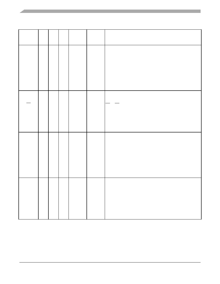
GPIOC6
(TA2)
(XB_IN3)
(CMP_REF)
21
23
31
Input/
Output
Input/
Output
Input
Analog
Input
Input,
internal
pullup
enabled
Port C GPIO — This GPIO pin can be individually programmed as
an input or output pin.
TA2 — Quad timer module A channel 2 input/output
XB_IN3 — Crossbar module input 3
CMP_REF— Positive input 3 of analog comparator A and B and C
After reset, the default state is GPIOC6
GPIOC7
(SS)
(TXD0)
22
24
32
Input/
Output
Input/
Output
Input,
internal
pullup
enabled
Port C GPIO — This GPIO pin can be individually programmed as
an input or output pin.
SS — SS is used in slave mode to indicate to the SPI module that
the current transfer is to be received.
TXD0 — SCI0 transmit data output or transmit/receive in single wire
operation
After reset, the default state is GPIOC7.
GPIOC8
(MISO)
(RXD0)
23
25
33
Input/
Output
Input/
Output
Input
Input,
internal
pullup
enabled
Port C GPIO — This GPIO pin can be individually programmed as
an input or output pin.
MISO — Master in/slave out. In master mode, this pin serves as the
data input. In slave mode, this pin serves as the data output. The
MISO line of a slave device is placed in the high-impedance state if
the slave device is not selected.
RXD0 — SCI0 receive data input
After reset, the default state is GPIOC8.
GPIOC9
(SCLK)
(XB_IN4)
24
26
34
Input/
Output
Input/
Output
Input
Input,
internal
pullup
enabled
Port C GPIO — This GPIO pin can be individually programmed as
an input or output pin.
SCLK — The SPI serial clock. In master mode, this pin serves as
an output, clocking slaved listeners. In slave mode, this pin serves
as the data clock input.
XB_IN4 — Crossbar module input 4
After reset, the default state is GPIOC9.
Table 5. MC56F825x/MC56F824x Signal and Package Information (continued)
Signal
Name
44
LQFP
48
LQFP
64
LQFP
Type
State
During
Reset
Signal Description
相关PDF资料 |
PDF描述 |
|---|---|
| VI-25B-IY-B1 | CONVERTER MOD DC/DC 95V 50W |
| S9S08DZ32F1MLF | MCU 32K FLASH MASK AUTO 48-LQFP |
| S9S08DZ60F1CLC | MCU 60K FLASH AUTO 32-LQFP |
| DS21552GN | IC TXRX T1 1-CHIP 5V 100-BGA |
| VE-B7Y-IY-B1 | CONVERTER MOD DC/DC 3.3V 33W |
相关代理商/技术参数 |
参数描述 |
|---|---|
| MC56F8257 | 制造商:FREESCALE 制造商全称:Freescale Semiconductor, Inc 功能描述:Digital Signal Controller Battery chargers and management |
| MC56F8257MLH | 功能描述:数字信号处理器和控制器 - DSP, DSC DSC 64 LQFP 64K FL RoHS:否 制造商:Microchip Technology 核心:dsPIC 数据总线宽度:16 bit 程序存储器大小:16 KB 数据 RAM 大小:2 KB 最大时钟频率:40 MHz 可编程输入/输出端数量:35 定时器数量:3 设备每秒兆指令数:50 MIPs 工作电源电压:3.3 V 最大工作温度:+ 85 C 封装 / 箱体:TQFP-44 安装风格:SMD/SMT |
| MC56F8257VLH | 功能描述:数字信号处理器和控制器 - DSP, DSC DSC 64 LQFP 64K FL RoHS:否 制造商:Microchip Technology 核心:dsPIC 数据总线宽度:16 bit 程序存储器大小:16 KB 数据 RAM 大小:2 KB 最大时钟频率:40 MHz 可编程输入/输出端数量:35 定时器数量:3 设备每秒兆指令数:50 MIPs 工作电源电压:3.3 V 最大工作温度:+ 85 C 封装 / 箱体:TQFP-44 安装风格:SMD/SMT |
| MC56F825X | 制造商:FREESCALE 制造商全称:Freescale Semiconductor, Inc 功能描述:Digital Signal Controller Battery chargers and management |
| MC56F82723VFM | 制造商:Freescale Semiconductor 功能描述:MC56F Series 100 MHz 32 KB Flash 3 KB SRAM 32-Bit Microcontroller - QFN-32 |
发布紧急采购,3分钟左右您将得到回复。