- 您现在的位置:买卖IC网 > PDF目录80565 > MC68302CPV16VC (FREESCALE SEMICONDUCTOR INC) 4 CHANNEL(S), 10M bps, LOCAL AREA NETWORK CONTROLLER, PQFP144 PDF资料下载
参数资料
| 型号: | MC68302CPV16VC |
| 厂商: | FREESCALE SEMICONDUCTOR INC |
| 元件分类: | 微控制器/微处理器 |
| 英文描述: | 4 CHANNEL(S), 10M bps, LOCAL AREA NETWORK CONTROLLER, PQFP144 |
| 封装: | 20 X 20 MM, 1.40 MM HEIGHT, 0.50 MM PITCH, PLASITC, LQFP-144 |
| 文件页数: | 127/128页 |
| 文件大小: | 641K |
| 代理商: | MC68302CPV16VC |
第1页第2页第3页第4页第5页第6页第7页第8页第9页第10页第11页第12页第13页第14页第15页第16页第17页第18页第19页第20页第21页第22页第23页第24页第25页第26页第27页第28页第29页第30页第31页第32页第33页第34页第35页第36页第37页第38页第39页第40页第41页第42页第43页第44页第45页第46页第47页第48页第49页第50页第51页第52页第53页第54页第55页第56页第57页第58页第59页第60页第61页第62页第63页第64页第65页第66页第67页第68页第69页第70页第71页第72页第73页第74页第75页第76页第77页第78页第79页第80页第81页第82页第83页第84页第85页第86页第87页第88页第89页第90页第91页第92页第93页第94页第95页第96页第97页第98页第99页第100页第101页第102页第103页第104页第105页第106页第107页第108页第109页第110页第111页第112页第113页第114页第115页第116页第117页第118页第119页第120页第121页第122页第123页第124页第125页第126页当前第127页第128页
IEEE 1149.1 (JTAG) Test Access Port
MOTOROLA
7-13
7.4.1 EXTEST
The external test (EXTEST) instruction selects the 163-bit boundary scan register.
By using the TAP, the register is capable of a) scanning user-defined values into the output
buffers, b) capturing values presented to input pins, c) controlling the direction of bidirec-
tional pins, and d) controlling the output drive of three-stateable output pins. For more details
on the function and use of EXTEST, refer to the IEEE 1149.1 document.
7.4.2 SAMPLE/PRELOAD
The SAMPLE/PRELOAD instruction provides two separate functions. First, it provides a
means to obtain a snapshot of system data and control signals. The snapshot occurs on the
rising edge of TCK in the capture-DR controller state. The data can be observed by shifting
it transparently through the boundary scan register.
NOTE
Since there is no internal synchronization between the scan
chain clock (TCK) and the system clock (CLKO), the user must
provide some form of external synchronization to achieve mean-
ingful results.
The second function of SAMPLE/PRELOAD is to initialize the boundary scan register output
cells prior to selection of EXTEST. This initialization ensures that known data will appear on
the outputs when entering the EXTEST instruction.
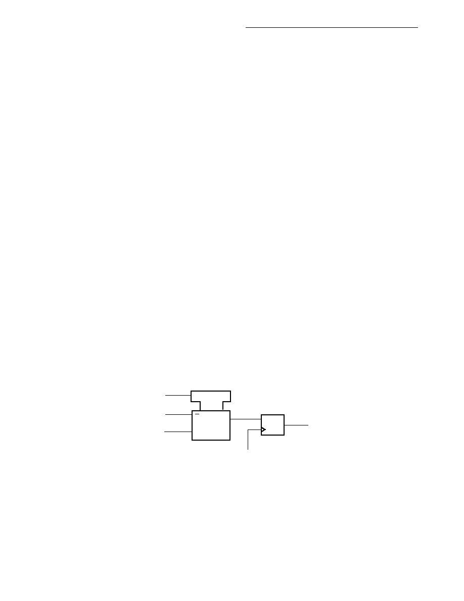
7.4.3 BYPASS
The BYPASS instruction selects the single-bit bypass register as shown in Figure 7-11. This
creates a shift register path from TDI to the bypass register and, finally, to TDO, circumvent-
ing the 163-bit boundary scan register. This instruction is used to enhance test efficiency
when a component other than the MC68EN302 becomes the device under test.
Figure 7-11. Bypass Register
When the bypass register is selected by the current instruction, the shift register stage is set
to a logic zero on the rising edge of TCK in the capture-DR controller state. Therefore, the
first bit to be shifted out after selecting the bypass register will always be a logic zero.
1
Mux
G1
C
D
TO TDO
FROM TDI
0
SHIFT DR
相关PDF资料 |
PDF描述 |
|---|---|
| MC68331CFC16B1 | 32-BIT, 16 MHz, MICROCONTROLLER, PQFP132 |
| MC68882CRC16A | 32-BIT, MATH COPROCESSOR, CPGA68 |
| MC68HC11E1VFN3 | 8-BIT, 3 MHz, MICROCONTROLLER, PQCC52 |
| MC68HC16Z1CFC25 | 16-BIT, 25.17 MHz, MICROCONTROLLER, PQFP132 |
| MC68HC705X32CFU4 | 8-BIT, OTPROM, 4 MHz, MICROCONTROLLER, PQFP64 |
相关代理商/技术参数 |
参数描述 |
|---|---|
| MC68302CRC16 | 制造商:MOTOROLA 制造商全称:Motorola, Inc 功能描述:Integrated Multiprotocol Processor User’s Manual |
| MC68302CRC16C | 功能描述:微处理器 - MPU 68K INTGR COM PROC DMA RoHS:否 制造商:Atmel 处理器系列:SAMA5D31 核心:ARM Cortex A5 数据总线宽度:32 bit 最大时钟频率:536 MHz 程序存储器大小:32 KB 数据 RAM 大小:128 KB 接口类型:CAN, Ethernet, LIN, SPI,TWI, UART, USB 工作电源电压:1.8 V to 3.3 V 最大工作温度:+ 85 C 安装风格:SMD/SMT 封装 / 箱体:FBGA-324 |
| MC68302CRC20 | 制造商:MOTOROLA 制造商全称:Motorola, Inc 功能描述:Integrated Multiprotocol Processor User’s Manual |
| MC68302CRC20C | 功能描述:微处理器 - MPU 68K INTGR COM PROC DMA RoHS:否 制造商:Atmel 处理器系列:SAMA5D31 核心:ARM Cortex A5 数据总线宽度:32 bit 最大时钟频率:536 MHz 程序存储器大小:32 KB 数据 RAM 大小:128 KB 接口类型:CAN, Ethernet, LIN, SPI,TWI, UART, USB 工作电源电压:1.8 V to 3.3 V 最大工作温度:+ 85 C 安装风格:SMD/SMT 封装 / 箱体:FBGA-324 |
发布紧急采购,3分钟左右您将得到回复。