- 您现在的位置:买卖IC网 > PDF目录45213 > MC68340RP16V (MOTOROLA INC) 32-BIT, 16.78 MHz, MICROCONTROLLER, PPGA145 PDF资料下载
参数资料
| 型号: | MC68340RP16V |
| 厂商: | MOTOROLA INC |
| 元件分类: | 微控制器/微处理器 |
| 英文描述: | 32-BIT, 16.78 MHz, MICROCONTROLLER, PPGA145 |
| 封装: | PLASTIC, PGA-145 |
| 文件页数: | 411/446页 |
| 文件大小: | 1800K |
| 代理商: | MC68340RP16V |
第1页第2页第3页第4页第5页第6页第7页第8页第9页第10页第11页第12页第13页第14页第15页第16页第17页第18页第19页第20页第21页第22页第23页第24页第25页第26页第27页第28页第29页第30页第31页第32页第33页第34页第35页第36页第37页第38页第39页第40页第41页第42页第43页第44页第45页第46页第47页第48页第49页第50页第51页第52页第53页第54页第55页第56页第57页第58页第59页第60页第61页第62页第63页第64页第65页第66页第67页第68页第69页第70页第71页第72页第73页第74页第75页第76页第77页第78页第79页第80页第81页第82页第83页第84页第85页第86页第87页第88页第89页第90页第91页第92页第93页第94页第95页第96页第97页第98页第99页第100页第101页第102页第103页第104页第105页第106页第107页第108页第109页第110页第111页第112页第113页第114页第115页第116页第117页第118页第119页第120页第121页第122页第123页第124页第125页第126页第127页第128页第129页第130页第131页第132页第133页第134页第135页第136页第137页第138页第139页第140页第141页第142页第143页第144页第145页第146页第147页第148页第149页第150页第151页第152页第153页第154页第155页第156页第157页第158页第159页第160页第161页第162页第163页第164页第165页第166页第167页第168页第169页第170页第171页第172页第173页第174页第175页第176页第177页第178页第179页第180页第181页第182页第183页第184页第185页第186页第187页第188页第189页第190页第191页第192页第193页第194页第195页第196页第197页第198页第199页第200页第201页第202页第203页第204页第205页第206页第207页第208页第209页第210页第211页第212页第213页第214页第215页第216页第217页第218页第219页第220页第221页第222页第223页第224页第225页第226页第227页第228页第229页第230页第231页第232页第233页第234页第235页第236页第237页第238页第239页第240页第241页第242页第243页第244页第245页第246页第247页第248页第249页第250页第251页第252页第253页第254页第255页第256页第257页第258页第259页第260页第261页第262页第263页第264页第265页第266页第267页第268页第269页第270页第271页第272页第273页第274页第275页第276页第277页第278页第279页第280页第281页第282页第283页第284页第285页第286页第287页第288页第289页第290页第291页第292页第293页第294页第295页第296页第297页第298页第299页第300页第301页第302页第303页第304页第305页第306页第307页第308页第309页第310页第311页第312页第313页第314页第315页第316页第317页第318页第319页第320页第321页第322页第323页第324页第325页第326页第327页第328页第329页第330页第331页第332页第333页第334页第335页第336页第337页第338页第339页第340页第341页第342页第343页第344页第345页第346页第347页第348页第349页第350页第351页第352页第353页第354页第355页第356页第357页第358页第359页第360页第361页第362页第363页第364页第365页第366页第367页第368页第369页第370页第371页第372页第373页第374页第375页第376页第377页第378页第379页第380页第381页第382页第383页第384页第385页第386页第387页第388页第389页第390页第391页第392页第393页第394页第395页第396页第397页第398页第399页第400页第401页第402页第403页第404页第405页第406页第407页第408页第409页第410页当前第411页第412页第413页第414页第415页第416页第417页第418页第419页第420页第421页第422页第423页第424页第425页第426页第427页第428页第429页第430页第431页第432页第433页第434页第435页第436页第437页第438页第439页第440页第441页第442页第443页第444页第445页第446页
3- 18
MC68340 USER’S MANUAL
MOTOROLA
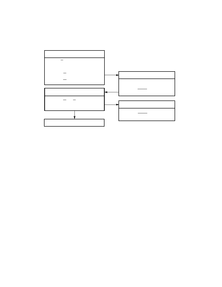
3.3.2 Write Cycle
During a write cycle, the MC68340 transfers data to memory or a peripheral device. Figure
3-8 is a flowchart of a word write cycle.
1. NEGATE DS AND AS
2. REMOVE DATA FROM D15–D0
BUS MASTER
SLAVE
ADDRESS DEVICE
1. SET R/W TO WRITE
2. DRIVE ADDRESS ON A31–A0
3. DRIVE FUNCTION CODE ON FC3–FC0
4. DRIVE SIZE PINS FOR OPERAND SIZE
5. ASSERT AS
6. PLACE DATA ON D15–D0
7. ASSERT DS
TERMINATE OUTPUT TRANSFER
START NEXT CYCLE
1. DECODE ADDRESS
2. LATCH DATA FROM D15–D0
ACCEPT DATA
3. ASSERT DSACKx SIGNALS
TERMINATE CYCLE
1. NEGATE DSACKx
Figure 3-8. Word Write Cycle Flowchart
State 0—The write cycle starts in S0. During S0, the MC68340 places a valid address on
A31–A0 and valid function codes on FC3–FC0. The function codes select the address
space for the cycle. The MC68340 drives R/
W low for a write cycle. SIZ1/SIZ0 become
valid, indicating the number of bytes to be transferred.
State 1—One-half clock later during S1, the MC68340 asserts
AS, indicating a valid
address on the address bus.
State 2—During S2, the MC68340 places the data to be written onto D15–D0, and
samples
DSACK
≈ at the end of S2.
State 3—The MC68340 asserts
DS during S3, indicating that data is stable on the data
bus. As long as at least one of the
DSACK
≈ signals is recognized by the end of S2
(meeting the asynchronous input setup time requirement), the cycle terminates one clock
later. If
DSACK
≈ is not recognized by the start of S3, the MC68340 inserts wait states
instead of proceeding to S4 and S5. To ensure that wait states are inserted, both
DSACK1 and DSACK0 must remain negated throughout the asynchronous input setup
and hold times around the end of S2. If wait states are added, the MC68340 continues to
sample
DSACK
≈ on the falling edges of the clock until one is recognized. The selected
device uses R/
W, SIZ1/SIZ0, and A0 to latch data from the appropriate byte(s) of D15–D8
and D7–D0. SIZ1/SIZ0 and A0 select the bytes of the data bus. If it has not already done
so, the device asserts
DSACK
≈ to signal that it has successfully stored the data.
相关PDF资料 |
PDF描述 |
|---|---|
| MC68340CPV16E | 32-BIT, 16.78 MHz, MICROCONTROLLER, PQFP144 |
| MC68340CFE16 | 32-BIT, 16.78 MHz, MICROCONTROLLER, CQFP144 |
| MC68341FT25 | 25.16 MHz, MICROPROCESSOR, PQFP160 |
| MC68341FT16V | 16.78 MHz, MICROPROCESSOR, PQFP160 |
| MC68360RC25VC | 32-BIT, 25 MHz, RISC MICROCONTROLLER, CPGA241 |
相关代理商/技术参数 |
参数描述 |
|---|---|
| MC68340RP25 | 制造商:FREESCALE 制造商全称:Freescale Semiconductor, Inc 功能描述:Integrated Processor with DMA User’s Manual |
| MC68340RP25B | 制造商:Motorola Inc 功能描述: |
| MC68340RP8V | 制造商:FREESCALE 制造商全称:Freescale Semiconductor, Inc 功能描述:Integrated Processor with DMA User’s Manual |
| MC68340UM/AD | 制造商:FREESCALE 制造商全称:Freescale Semiconductor, Inc 功能描述:Product Brief Integrated Processor With DMA |
| MC68340UMAD | 制造商:FREESCALE 制造商全称:Freescale Semiconductor, Inc 功能描述:Integrated Processor with DMA Usera??s Manual |
发布紧急采购,3分钟左右您将得到回复。