- 您现在的位置:买卖IC网 > PDF目录45235 > MC68HC05B16FNR2 (FREESCALE SEMICONDUCTOR INC) 8-BIT, MROM, 2.1 MHz, MICROCONTROLLER, PQCC52 PDF资料下载
参数资料
| 型号: | MC68HC05B16FNR2 |
| 厂商: | FREESCALE SEMICONDUCTOR INC |
| 元件分类: | 微控制器/微处理器 |
| 英文描述: | 8-BIT, MROM, 2.1 MHz, MICROCONTROLLER, PQCC52 |
| 封装: | PLASTIC, LCC-52 |
| 文件页数: | 121/298页 |
| 文件大小: | 3532K |
| 代理商: | MC68HC05B16FNR2 |
第1页第2页第3页第4页第5页第6页第7页第8页第9页第10页第11页第12页第13页第14页第15页第16页第17页第18页第19页第20页第21页第22页第23页第24页第25页第26页第27页第28页第29页第30页第31页第32页第33页第34页第35页第36页第37页第38页第39页第40页第41页第42页第43页第44页第45页第46页第47页第48页第49页第50页第51页第52页第53页第54页第55页第56页第57页第58页第59页第60页第61页第62页第63页第64页第65页第66页第67页第68页第69页第70页第71页第72页第73页第74页第75页第76页第77页第78页第79页第80页第81页第82页第83页第84页第85页第86页第87页第88页第89页第90页第91页第92页第93页第94页第95页第96页第97页第98页第99页第100页第101页第102页第103页第104页第105页第106页第107页第108页第109页第110页第111页第112页第113页第114页第115页第116页第117页第118页第119页第120页当前第121页第122页第123页第124页第125页第126页第127页第128页第129页第130页第131页第132页第133页第134页第135页第136页第137页第138页第139页第140页第141页第142页第143页第144页第145页第146页第147页第148页第149页第150页第151页第152页第153页第154页第155页第156页第157页第158页第159页第160页第161页第162页第163页第164页第165页第166页第167页第168页第169页第170页第171页第172页第173页第174页第175页第176页第177页第178页第179页第180页第181页第182页第183页第184页第185页第186页第187页第188页第189页第190页第191页第192页第193页第194页第195页第196页第197页第198页第199页第200页第201页第202页第203页第204页第205页第206页第207页第208页第209页第210页第211页第212页第213页第214页第215页第216页第217页第218页第219页第220页第221页第222页第223页第224页第225页第226页第227页第228页第229页第230页第231页第232页第233页第234页第235页第236页第237页第238页第239页第240页第241页第242页第243页第244页第245页第246页第247页第248页第249页第250页第251页第252页第253页第254页第255页第256页第257页第258页第259页第260页第261页第262页第263页第264页第265页第266页第267页第268页第269页第270页第271页第272页第273页第274页第275页第276页第277页第278页第279页第280页第281页第282页第283页第284页第285页第286页第287页第288页第289页第290页第291页第292页第293页第294页第295页第296页第297页第298页
MC68HC05B6
Rev. 4
MOTOROLA
E-19
MC68HC705B16
14
E.4.4
RAM parallel bootstrap
The program rst checks the state of the security bit. If the SEC bit is active, i.e. ‘0’, the program
will not enter the RAM bootstrap mode and the red LED will ash. Otherwise the RAM bootstrap
program will start loading the RAM with external data (e.g. from a 2564 or 2764 EPROM). Before
loading a new byte the state of the PD4/AN4 pin is checked. If this pin goes to level ‘0’, or if the
RAM is full, then control is given to the loaded program at address $0050. See Figure E-3 and
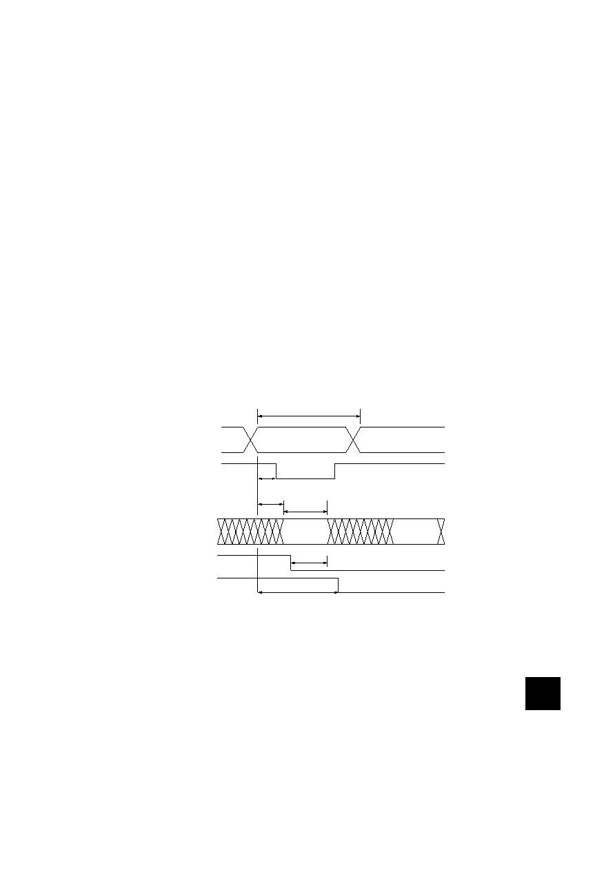
If the data is supplied by a parallel interface, handshaking will be provided by PC5 and PC6
according to Figure E-9. If the data comes from an external EPROM, the handshake can be
disabled by connecting together PC5 and PC6.
Figure E-10 provides a schematic diagram of a circuit that can be used to load the RAM with short
test programs. Up to 8 programs can be loaded in turn from the EPROM. Selection is
accomplished by means of the switches connected to the EPROM higher address lines (A8
through A10). If the user program sets PC0 to level ‘1’, this will disable the external EPROM, thus
rendering both port A output and port B input available. The EPROM parallel bootstrap loader
lines will be at zero. The LEDs will stay off.
Figure E-9 Parallel RAM loader timing diagram
tADR
tDHR
Address
Data
tCR
PD4
tEXR max
tHO
tHI max
PC5 out
PC6 in
tADR max (address to data delay; PC6=PC5)
16 machine cycles
tDHR min (data hold time)
4 machine cycles
tCR (load cycle time; PC6=PC5)
49 machine cycles
tHO (PC5 handshake out delay)
5 machine cycles
tHI max (PC6 handshake in, data hold time)
10 machine cycles
tEXR max (max delay for transition to be recognised during this cycle; PC6=PC5
30 machine cycles
1 machine cycle = 1/(2f0(Xtal))
TPG
203
05B6Book Page 19 Tuesday, April 6, 1999 8:24 am
相关PDF资料 |
PDF描述 |
|---|---|
| MC68HC05B16CFNR2 | 8-BIT, MROM, 2.1 MHz, MICROCONTROLLER, PQCC52 |
| MC68HC05B4FNR2 | 8-BIT, MROM, 2.1 MHz, MICROCONTROLLER, PQCC52 |
| MC68HC705B16NB | 8-BIT, OTPROM, MICROCONTROLLER, PDIP56 |
| MC68HC705B16FNR2 | 8-BIT, OTPROM, 2.1 MHz, MICROCONTROLLER, PQCC52 |
| MC68HC705B16NVFU | 8-BIT, OTPROM, 2.1 MHz, MICROCONTROLLER, PQFP64 |
相关代理商/技术参数 |
参数描述 |
|---|---|
| MC68HC05B32 | 制造商:FREESCALE 制造商全称:Freescale Semiconductor, Inc 功能描述:Microcontrollers |
| MC68HC05B4 | 制造商:FREESCALE 制造商全称:Freescale Semiconductor, Inc 功能描述:Microcontrollers |
| MC68HC05B4_05 | 制造商:FREESCALE 制造商全称:Freescale Semiconductor, Inc 功能描述:Microcontrollers |
| MC68HC05B5 | 制造商:FREESCALE 制造商全称:Freescale Semiconductor, Inc 功能描述:Microcontrollers |
| MC68HC05B6 | 制造商:FREESCALE 制造商全称:Freescale Semiconductor, Inc 功能描述:Microcontrollers |
发布紧急采购,3分钟左右您将得到回复。