- 您现在的位置:买卖IC网 > PDF目录102741 > MC68HC11P2BCFN4 (ABILIS SYSTEMS) 8-BIT, MROM, 4 MHz, MICROCONTROLLER, PQCC84 PDF资料下载
参数资料
| 型号: | MC68HC11P2BCFN4 |
| 厂商: | ABILIS SYSTEMS |
| 元件分类: | 微控制器/微处理器 |
| 英文描述: | 8-BIT, MROM, 4 MHz, MICROCONTROLLER, PQCC84 |
| 封装: | PLASTIC, LCC-84 |
| 文件页数: | 147/268页 |
| 文件大小: | 2325K |
| 代理商: | MC68HC11P2BCFN4 |
第1页第2页第3页第4页第5页第6页第7页第8页第9页第10页第11页第12页第13页第14页第15页第16页第17页第18页第19页第20页第21页第22页第23页第24页第25页第26页第27页第28页第29页第30页第31页第32页第33页第34页第35页第36页第37页第38页第39页第40页第41页第42页第43页第44页第45页第46页第47页第48页第49页第50页第51页第52页第53页第54页第55页第56页第57页第58页第59页第60页第61页第62页第63页第64页第65页第66页第67页第68页第69页第70页第71页第72页第73页第74页第75页第76页第77页第78页第79页第80页第81页第82页第83页第84页第85页第86页第87页第88页第89页第90页第91页第92页第93页第94页第95页第96页第97页第98页第99页第100页第101页第102页第103页第104页第105页第106页第107页第108页第109页第110页第111页第112页第113页第114页第115页第116页第117页第118页第119页第120页第121页第122页第123页第124页第125页第126页第127页第128页第129页第130页第131页第132页第133页第134页第135页第136页第137页第138页第139页第140页第141页第142页第143页第144页第145页第146页当前第147页第148页第149页第150页第151页第152页第153页第154页第155页第156页第157页第158页第159页第160页第161页第162页第163页第164页第165页第166页第167页第168页第169页第170页第171页第172页第173页第174页第175页第176页第177页第178页第179页第180页第181页第182页第183页第184页第185页第186页第187页第188页第189页第190页第191页第192页第193页第194页第195页第196页第197页第198页第199页第200页第201页第202页第203页第204页第205页第206页第207页第208页第209页第210页第211页第212页第213页第214页第215页第216页第217页第218页第219页第220页第221页第222页第223页第224页第225页第226页第227页第228页第229页第230页第231页第232页第233页第234页第235页第236页第237页第238页第239页第240页第241页第242页第243页第244页第245页第246页第247页第248页第249页第250页第251页第252页第253页第254页第255页第256页第257页第258页第259页第260页第261页第262页第263页第264页第265页第266页第267页第268页
CPU Core and Instruction Set
Technical Data
MC68HC11P2 — Rev 1.0
CPU Core and Instruction Set
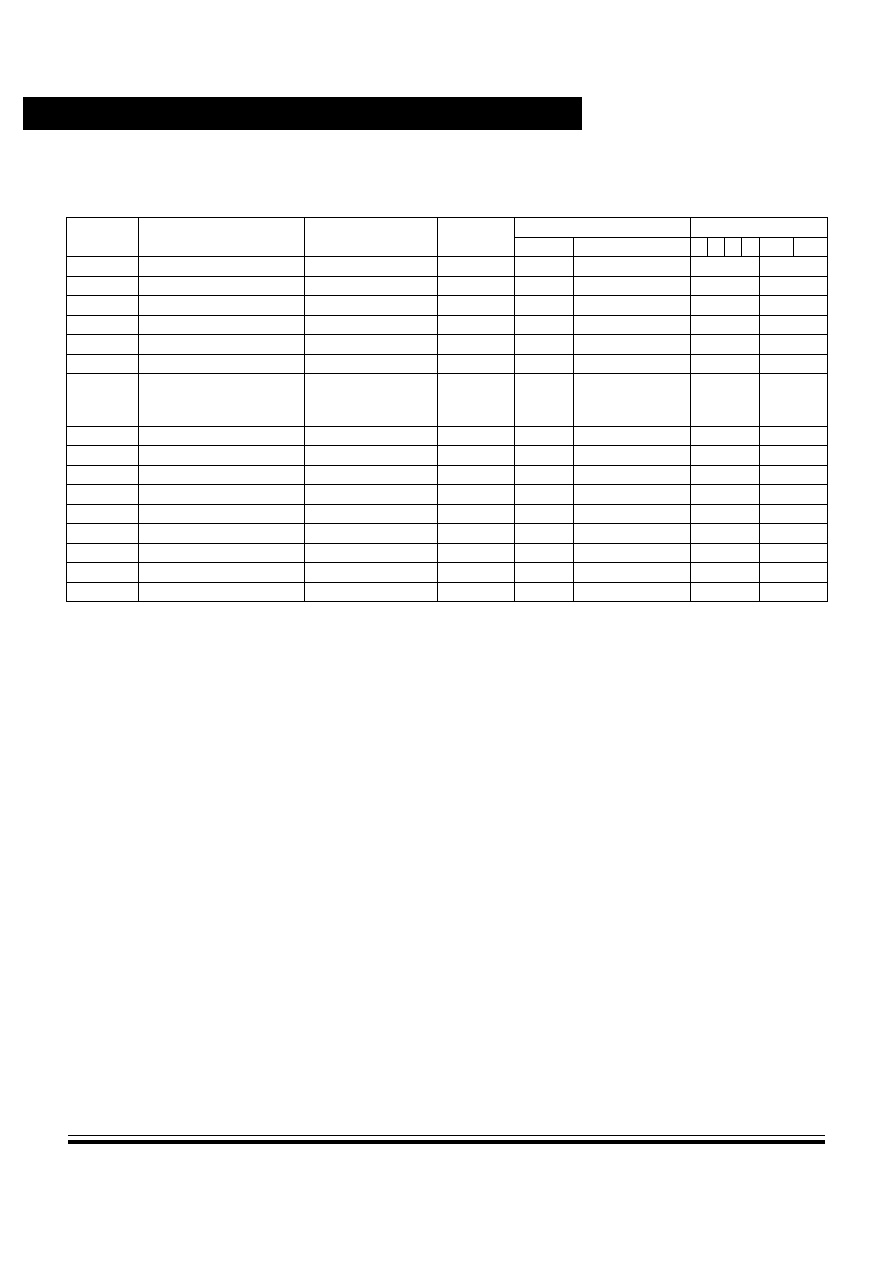
SWI
Software interrupt
see Figure 11-2
INH
3F
—
14
—— — 1 —— ——
TAB
Transfer A to B
A
BINH
16
—
2
—— ——
0 —
TAP
Transfer A to CC register
A
CCR
INH
06
—
2
↓
TBA
Transfer B to A
B
AINH
17
—
2
—— ——
0 —
TEST
Test (only in test modes)
address bus increments
INH
00
—
—— —— —— ——
TPA
Transfer CC register to A
CCR
AINH
07
—
2
—— —— —— ——
TST (opr)
Test for zero or minus
M – 0
EXT
IND, X
IND, Y
7D
6D
18 6D
hh ll
ff
6
7
—— ——
00
TSTA
Test A for zero or minus
A – 0
A INH
4D
—
2
—— ——
00
TSTB
Test B for zero or minus
B – 0
B INH
5D
—
2
—— ——
00
TSX
Transfer stack pointer to X
SP + 1
IX
INH
30
—
3
—— —— —— ——
TSY
Transfer stack pointer to Y
SP + 1
IY
INH
18 30
—
4
—— —— —— ——
TXS
Transfer X to stack pointer
IX – 1
SP
INH
35
—
3
—— —— —— ——
TYS
Transfer Y to stack pointer
IY – 1
SP
INH
18 35
—
4
—— —— —— ——
WAI
Wait for interrupt
stack registers & WAIT
INH
3E
—
—— —— —— ——
XGDX
Exchange D with X
IX
D; D IX
INH
8F
—
3
—— —— —— ——
XGDY
Exchange D with Y
IY
D; D IY
INH
18 8F
—
4
—— —— —— ——
Operators
Operands
Is transferred to
dd
8-bit direct address ($0000–$00FF); the high byte is assumed
Boolean AND
to be zero
+ Arithmetic addition, except where used as an
ff
8-bit positive offset ($00 to $FF (0 to 256)) is added to the
inclusive-OR symbol in Boolean formulae
contents of the index register
⊕ Exclusive-OR
hh
High order byte of 16-bit extended address
* Multiply
ii
One byte of immediate data
: Concatenation
jj
High order byte of 16-bit immediate data
– Arithmetic subtraction, or negation symbol
kk
Low order byte of 16-bit immediate data
(Twos complement)
ll
Low order byte of 16-bit extended address
mm 8-bit mask (set bits to be affected)
rr
Signed relative offset ($80 to $7F (–128 to +127));
offset is relative to the address following the offset byte
Cycles
Condition Codes
Infinite, or until reset occurs
—
Bit not changed
12 cycles are used, beginning with the opcode
0
Bit always cleared
fetch. A wait state is entered, which remains
1
Bit always set
in effect for an integer number of MPU E clock
Bit set or cleared, depending on the operation
cycles (n) until an interrupt is recognized.
↓
Bit can be cleared, but cannot become set
Finally, two additional cycles are used to fetch
?
Not defined
the appropriate interrupt vector. (14 + n, total).
Table 11-2. Instruction set (Sheet 8 of 8)
Mnemonic
Operation
Description
Addressing
mode
Instruction
Condition codes
Opcode
Operand
Cycles
S X H I N Z V C
F
re
e
sc
a
le
S
e
m
ic
o
n
d
u
c
to
r,
I
Freescale Semiconductor, Inc.
For More Information On This Product,
Go to: www.freescale.com
n
c
..
.
相关PDF资料 |
PDF描述 |
|---|---|
| M30263F3AFP | 16-BIT, FLASH, 20 MHz, MICROCONTROLLER, PDSO42 |
| M30281FCBHP-U7 | 16-BIT, FLASH, 24 MHz, MICROCONTROLLER, PQFP64 |
| M30290FCTHP | 16-BIT, FLASH, 20 MHz, MICROCONTROLLER, PQFP80 |
| M30623MCT-XXXGP | 16-BIT, MROM, 16 MHz, MICROCONTROLLER, PQFP80 |
| M30624MHP-XXXFP | 16-BIT, MROM, 24 MHz, MICROCONTROLLER, PQFP100 |
相关代理商/技术参数 |
参数描述 |
|---|---|
| MC68HC16Z1CAG | 制造商:Freescale Semiconductor 功能描述: |
| MC68HC16Z1CAG16 | 功能描述:16位微控制器 - MCU 16 BIT MCU 1K RAM RoHS:否 制造商:Texas Instruments 核心:RISC 处理器系列:MSP430FR572x 数据总线宽度:16 bit 最大时钟频率:24 MHz 程序存储器大小:8 KB 数据 RAM 大小:1 KB 片上 ADC:Yes 工作电源电压:2 V to 3.6 V 工作温度范围:- 40 C to + 85 C 封装 / 箱体:VQFN-40 安装风格:SMD/SMT |
| MC68HC16Z1CAG16 | 制造商:Freescale Semiconductor 功能描述:IC16-BIT MICROCONTROLLER |
| MC68HC16Z1CAG20 | 功能描述:16位微控制器 - MCU 16 BIT MCU 1K RAM RoHS:否 制造商:Texas Instruments 核心:RISC 处理器系列:MSP430FR572x 数据总线宽度:16 bit 最大时钟频率:24 MHz 程序存储器大小:8 KB 数据 RAM 大小:1 KB 片上 ADC:Yes 工作电源电压:2 V to 3.6 V 工作温度范围:- 40 C to + 85 C 封装 / 箱体:VQFN-40 安装风格:SMD/SMT |
| MC68HC16Z1CAG20 | 制造商:Freescale Semiconductor 功能描述:Microcontroller |
发布紧急采购,3分钟左右您将得到回复。