- 您现在的位置:买卖IC网 > PDF目录80479 > MC68HC811E2MP2 (FREESCALE SEMICONDUCTOR INC) 8-BIT, EEPROM, 2 MHz, MICROCONTROLLER, PDIP48 PDF资料下载
参数资料
| 型号: | MC68HC811E2MP2 |
| 厂商: | FREESCALE SEMICONDUCTOR INC |
| 元件分类: | 微控制器/微处理器 |
| 英文描述: | 8-BIT, EEPROM, 2 MHz, MICROCONTROLLER, PDIP48 |
| 封装: | DIP-48 |
| 文件页数: | 37/242页 |
| 文件大小: | 1672K |
| 代理商: | MC68HC811E2MP2 |
第1页第2页第3页第4页第5页第6页第7页第8页第9页第10页第11页第12页第13页第14页第15页第16页第17页第18页第19页第20页第21页第22页第23页第24页第25页第26页第27页第28页第29页第30页第31页第32页第33页第34页第35页第36页当前第37页第38页第39页第40页第41页第42页第43页第44页第45页第46页第47页第48页第49页第50页第51页第52页第53页第54页第55页第56页第57页第58页第59页第60页第61页第62页第63页第64页第65页第66页第67页第68页第69页第70页第71页第72页第73页第74页第75页第76页第77页第78页第79页第80页第81页第82页第83页第84页第85页第86页第87页第88页第89页第90页第91页第92页第93页第94页第95页第96页第97页第98页第99页第100页第101页第102页第103页第104页第105页第106页第107页第108页第109页第110页第111页第112页第113页第114页第115页第116页第117页第118页第119页第120页第121页第122页第123页第124页第125页第126页第127页第128页第129页第130页第131页第132页第133页第134页第135页第136页第137页第138页第139页第140页第141页第142页第143页第144页第145页第146页第147页第148页第149页第150页第151页第152页第153页第154页第155页第156页第157页第158页第159页第160页第161页第162页第163页第164页第165页第166页第167页第168页第169页第170页第171页第172页第173页第174页第175页第176页第177页第178页第179页第180页第181页第182页第183页第184页第185页第186页第187页第188页第189页第190页第191页第192页第193页第194页第195页第196页第197页第198页第199页第200页第201页第202页第203页第204页第205页第206页第207页第208页第209页第210页第211页第212页第213页第214页第215页第216页第217页第218页第219页第220页第221页第222页第223页第224页第225页第226页第227页第228页第229页第230页第231页第232页第233页第234页第235页第236页第237页第238页第239页第240页第241页第242页
Input Capture
M68HC11E Family Data Sheet, Rev. 5.1
Freescale Semiconductor
131
The control and status bits that implement the input capture functions are contained in:
Pulse accumulator control register (PACTL)
Timer control 2 register (TCTL2)
Timer interrupt mask 1 register (TMSK1)
Timer interrupt flag 2 register (TFLG1)
To configure port A bit 3 as an input capture, clear the DDRA3 bit of the PACTL register. Note that this bit
is cleared out of reset. To enable PA3 as the fourth input capture, set the I4/O5 bit in the PACTL register.
Otherwise, PA3 is configured as a fifth output compare out of reset, with bit I4/O5 being cleared. If the
DDRA3 bit is set (configuring PA3 as an output), and IC4 is enabled, then writes to PA3 cause edges on
the pin to result in input captures. Writing to TI4/O5 has no effect when the TI4/O5 register is acting as IC4.
9.3.1 Timer Control Register 2
Use the control bits of this register to program input capture functions to detect a particular edge polarity
on the corresponding timer input pin. Each of the input capture functions can be independently configured
to detect rising edges only, falling edges only, any edge (rising or falling), or to disable the input capture
function. The input capture functions operate independently of each other and can capture the same
TCNT value if the input edges are detected within the same timer count cycle.
EDGxB and EDGxA — Input Capture Edge Control Bits
There are four pairs of these bits. Each pair is cleared to 0 by reset and must be encoded to configure
the corresponding input capture edge detector circuit. IC4 functions only if the I4/O5 bit in the PACTL
register is set. Refer to Table 9-2 for timer control configuration.
9.3.2 Timer Input Capture Registers
When an edge has been detected and synchronized, the 16-bit free-running counter value is transferred
into the input capture register pair as a single 16-bit parallel transfer. Timer counter value captures and
timer counter incrementing occur on opposite half-cycles of the phase 2 clock so that the count value is
stable whenever a capture occurs. The timer input capture registers are not affected by reset. Input
capture values can be read from a pair of 8-bit read-only registers. A read of the high-order byte of an
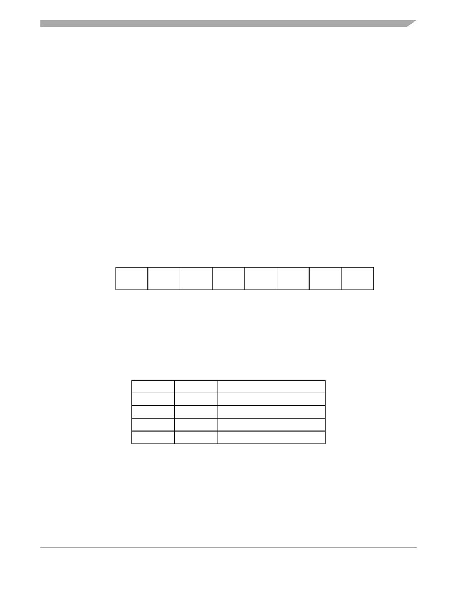
Address:
$1021
Bit 7
654321
Bit 0
Read:
EDG4B
EDG4A
EDG1B
EDG1A
EDG2B
EDG2A
EDG3B
EDG3A
Write:
Reset:
00000000
Figure 9-3. Timer Control Register 2 (TCTL2)
Table 9-2. Timer Control Configuration
EDGxB
EDGxA
Configuration
0
Capture disabled
0
1
Capture on rising edges only
1
0
Capture on falling edges only
1
Capture on any edge
相关PDF资料 |
PDF描述 |
|---|---|
| MC68HC908QT1MDW | 8-BIT, FLASH, 8 MHz, MICROCONTROLLER, PDSO8 |
| MC68020FC25E | 32-BIT, 25 MHz, MICROPROCESSOR, PQFP132 |
| MC68332AMPV20 | 32-BIT, 20 MHz, MICROCONTROLLER, PQFP144 |
| MC68340CFT16E | 32-BIT, 16.78 MHz, MICROCONTROLLER, PQFP144 |
| MC68360ZP33L | 4 CHANNEL(S), 10M bps, LOCAL AREA NETWORK CONTROLLER, PBGA357 |
相关代理商/技术参数 |
参数描述 |
|---|---|
| MC68HC908AB32CFU | 功能描述:IC MCU 8MHZ 32K FLASH 64-QFP RoHS:否 类别:集成电路 (IC) >> 嵌入式 - 微控制器, 系列:HC08 其它有关文件:STM32F101T8 View All Specifications 特色产品:STM32 32-bit Cortex MCUs 标准包装:490 系列:STM32 F1 核心处理器:ARM? Cortex?-M3 芯体尺寸:32-位 速度:36MHz 连通性:I²C,IrDA,LIN,SPI,UART/USART 外围设备:DMA,PDR,POR,PVD,PWM,温度传感器,WDT 输入/输出数:26 程序存储器容量:64KB(64K x 8) 程序存储器类型:闪存 EEPROM 大小:- RAM 容量:10K x 8 电压 - 电源 (Vcc/Vdd):2 V ~ 3.6 V 数据转换器:A/D 10x12b 振荡器型:内部 工作温度:-40°C ~ 85°C 封装/外壳:36-VFQFN,36-VFQFPN 包装:托盘 配用:497-10030-ND - STARTER KIT FOR STM32497-8853-ND - BOARD DEMO STM32 UNIV USB-UUSCIKSDKSTM32-PL-ND - KIT IAR KICKSTART STM32 CORTEXM3497-8512-ND - KIT STARTER FOR STM32F10XE MCU497-8505-ND - KIT STARTER FOR STM32F10XE MCU497-8304-ND - KIT STM32 MOTOR DRIVER BLDC497-6438-ND - BOARD EVALUTION FOR STM32 512K497-6289-ND - KIT PERFORMANCE STICK FOR STM32MCBSTM32UME-ND - BOARD EVAL MCBSTM32 + ULINK-MEMCBSTM32U-ND - BOARD EVAL MCBSTM32 + ULINK2更多... 其它名称:497-9032STM32F101T8U6-ND |
| MC68HC908AB32MFU | 制造商:Rochester Electronics LLC 功能描述:32K FLASH & 512 EE - Bulk |
| MC68HC908AB32MPB | 功能描述:IC MCU 32K FLASH 8MHZ 64-LQFP RoHS:否 类别:集成电路 (IC) >> 嵌入式 - 微控制器, 系列:HC08 标准包装:250 系列:56F8xxx 核心处理器:56800E 芯体尺寸:16-位 速度:60MHz 连通性:CAN,SCI,SPI 外围设备:POR,PWM,温度传感器,WDT 输入/输出数:21 程序存储器容量:40KB(20K x 16) 程序存储器类型:闪存 EEPROM 大小:- RAM 容量:6K x 16 电压 - 电源 (Vcc/Vdd):2.25 V ~ 3.6 V 数据转换器:A/D 6x12b 振荡器型:内部 工作温度:-40°C ~ 125°C 封装/外壳:48-LQFP 包装:托盘 配用:MC56F8323EVME-ND - BOARD EVALUATION MC56F8323 |
| MC68HC908AP16CB | 功能描述:IC MCU 16K FLASH 8MHZ 42SDIP RoHS:否 类别:集成电路 (IC) >> 嵌入式 - 微控制器, 系列:HC08 标准包装:250 系列:56F8xxx 核心处理器:56800E 芯体尺寸:16-位 速度:60MHz 连通性:CAN,SCI,SPI 外围设备:POR,PWM,温度传感器,WDT 输入/输出数:21 程序存储器容量:40KB(20K x 16) 程序存储器类型:闪存 EEPROM 大小:- RAM 容量:6K x 16 电压 - 电源 (Vcc/Vdd):2.25 V ~ 3.6 V 数据转换器:A/D 6x12b 振荡器型:内部 工作温度:-40°C ~ 125°C 封装/外壳:48-LQFP 包装:托盘 配用:MC56F8323EVME-ND - BOARD EVALUATION MC56F8323 |
| MC68HC908AP16CBE | 制造商:Freescale Semiconductor 功能描述: |
发布紧急采购,3分钟左右您将得到回复。