- 您现在的位置:买卖IC网 > PDF目录45240 > MC68HC908EY16AMFA (FREESCALE SEMICONDUCTOR INC) 8-BIT, FLASH, 8 MHz, MICROCONTROLLER, PQFP32 PDF资料下载
参数资料
| 型号: | MC68HC908EY16AMFA |
| 厂商: | FREESCALE SEMICONDUCTOR INC |
| 元件分类: | 微控制器/微处理器 |
| 英文描述: | 8-BIT, FLASH, 8 MHz, MICROCONTROLLER, PQFP32 |
| 封装: | 7 X 7 MM, 1.40 MM HEIGHT, 0.80 MM PITCH, MS-026BBA, LQFP-32 |
| 文件页数: | 211/292页 |
| 文件大小: | 1990K |
| 代理商: | MC68HC908EY16AMFA |
第1页第2页第3页第4页第5页第6页第7页第8页第9页第10页第11页第12页第13页第14页第15页第16页第17页第18页第19页第20页第21页第22页第23页第24页第25页第26页第27页第28页第29页第30页第31页第32页第33页第34页第35页第36页第37页第38页第39页第40页第41页第42页第43页第44页第45页第46页第47页第48页第49页第50页第51页第52页第53页第54页第55页第56页第57页第58页第59页第60页第61页第62页第63页第64页第65页第66页第67页第68页第69页第70页第71页第72页第73页第74页第75页第76页第77页第78页第79页第80页第81页第82页第83页第84页第85页第86页第87页第88页第89页第90页第91页第92页第93页第94页第95页第96页第97页第98页第99页第100页第101页第102页第103页第104页第105页第106页第107页第108页第109页第110页第111页第112页第113页第114页第115页第116页第117页第118页第119页第120页第121页第122页第123页第124页第125页第126页第127页第128页第129页第130页第131页第132页第133页第134页第135页第136页第137页第138页第139页第140页第141页第142页第143页第144页第145页第146页第147页第148页第149页第150页第151页第152页第153页第154页第155页第156页第157页第158页第159页第160页第161页第162页第163页第164页第165页第166页第167页第168页第169页第170页第171页第172页第173页第174页第175页第176页第177页第178页第179页第180页第181页第182页第183页第184页第185页第186页第187页第188页第189页第190页第191页第192页第193页第194页第195页第196页第197页第198页第199页第200页第201页第202页第203页第204页第205页第206页第207页第208页第209页第210页当前第211页第212页第213页第214页第215页第216页第217页第218页第219页第220页第221页第222页第223页第224页第225页第226页第227页第228页第229页第230页第231页第232页第233页第234页第235页第236页第237页第238页第239页第240页第241页第242页第243页第244页第245页第246页第247页第248页第249页第250页第251页第252页第253页第254页第255页第256页第257页第258页第259页第260页第261页第262页第263页第264页第265页第266页第267页第268页第269页第270页第271页第272页第273页第274页第275页第276页第277页第278页第279页第280页第281页第282页第283页第284页第285页第286页第287页第288页第289页第290页第291页第292页
Monitor Mode
MC68HC908EY16A MC68HC908EY8A Data Sheet, Rev. 0
Freescale Semiconductor
289
Enabling an ADC channel no longer overrides the digital I/O function of the associated pin. To
prevent the digital I/O from interfering with the ADC read of the pin, the data direction bit associated
with the port pin must be set as input.
B.3 Monitor Mode
B.3.1 Monitor Extended Security
An extended security feature has been added to the 908EY16 monitor operation. When the extended
security location is programmed with zero and all 8 byte security matches, the monitor is terminated in an
infinite loop automatically. To unlock extended security, the part must enter monitor mode with failed
security and then the FLASH must be mass-erased to erase the whole FLASH. The extended security
location in the 908EY16A is located at address $FDFF. The user should check this location in their
software to ensure that it will not cause unexpected operation.
B.3.2 Zeroes in Security Bytes
An additional check has been added to the verification of the security bytes. The number of zero bytes
used for the security bytes is limited to 5. More than 5 bytes of zero out of the 8 security bytes will cause
the security check to fail. The user should check the values programmed into locations $FFF6–$FFFD to
ensure that this requirement is not violated.
B.3.3 Forced Monitor Mode Baud Rate
The baud rate used for the 908EY16 Forced Monitor Mode was set at ~6300 baud. In the 908EY16A, this
has been changed to 9600 baud. In addition, the trim value stored in FLASH is used in this mode to ensure
that the tolerance required for communicating at this rate is met.
B.4 Monitor ROM FLASH Programming Routines
B.4.1 Erase
The existing 908EY16 call for erase uses a RAM variable called CTRLBYT to determine whether the call
is for page or mass erase. The 908EY16A routine uses the address passed to determine the page to be
erased. (If ADDR = FLBPR, then a mass erase is performed.) If the parameters for the current 908EY16
routine are passed to the new 908EY16A routine for a page erase, it would work correctly. Using an
existing 908EY16 call to mass erase the 908EY16A will not work.
A minor difference is that the new 908EY16A routine preserves the original state of the I bit while the
existing 908EY16 erase routine sets the I bit and leaves it set on exit.
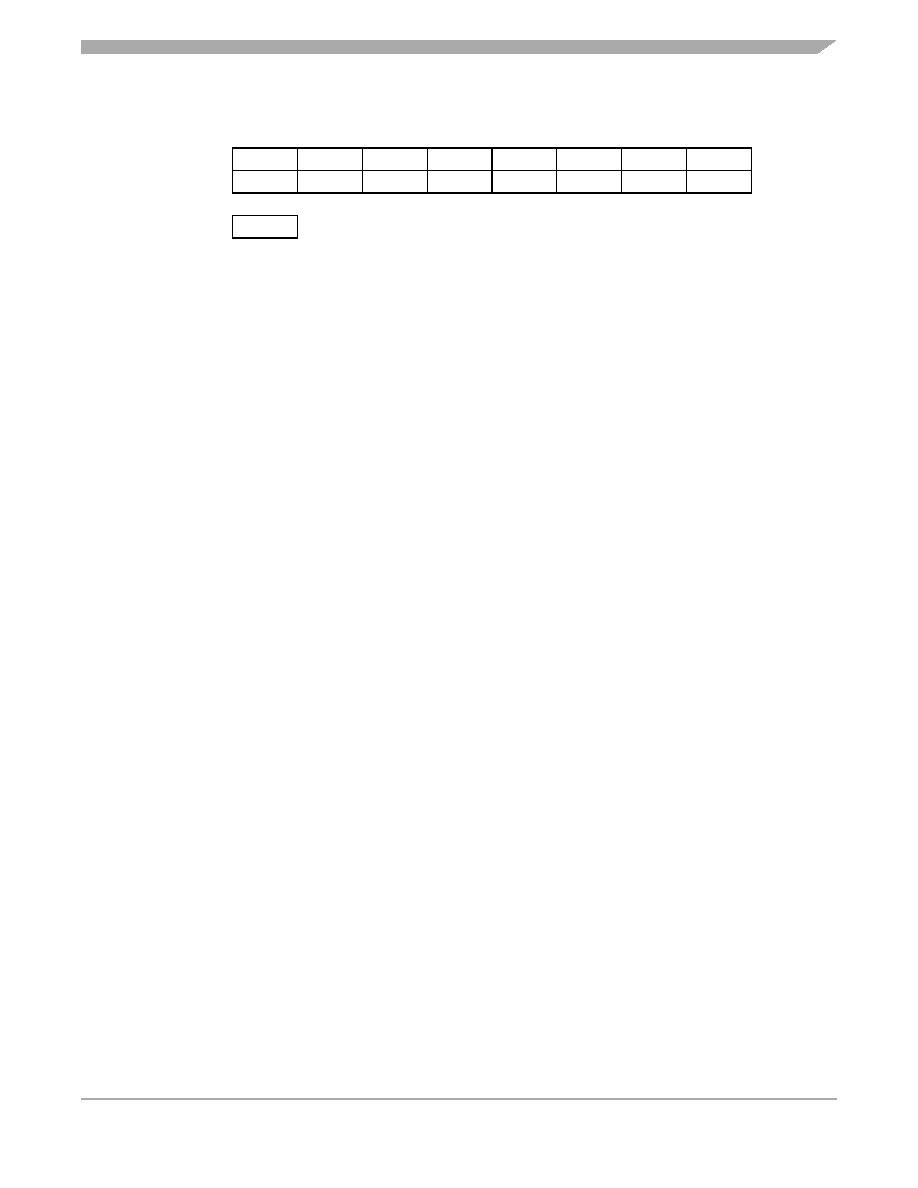
Address:
$003F
Bit 7
6
5
4321
Bit 0
908EY16:
ADIV2
ADIV1
ADIV0
ADICLK
MODE1
MODE0
R
0/NA
908EY16A:
ADLPC
ADIV1
ADIV0
ADICLK
MODE1
MODE0
ADLSMP
ACLKEN
Reset:
000
00000
R= Reserved
Figure B-4. ADC10 Clock Register (ADCLK)
相关PDF资料 |
PDF描述 |
|---|---|
| MC68HC908EY8AVFA | 8-BIT, FLASH, 8 MHz, MICROCONTROLLER, PQFP32 |
| MC68HC908EY8AMFA | 8-BIT, FLASH, 8 MHz, MICROCONTROLLER, PQFP32 |
| MC68HC908EY16AMFAE | 8-BIT, FLASH, 8 MHz, MICROCONTROLLER, PQFP32 |
| MC68HC908EY8KFA | 8-BIT, FLASH, 8 MHz, MICROCONTROLLER, PQFP32 |
| MC68HC908EY16MFAE | 8-BIT, FLASH, 8 MHz, MICROCONTROLLER, PQFP32 |
相关代理商/技术参数 |
参数描述 |
|---|---|
| MC68HC908EY16CFA | 功能描述:8位微控制器 -MCU 8BIT MCU 16K FLASH RoHS:否 制造商:Silicon Labs 核心:8051 处理器系列:C8051F39x 数据总线宽度:8 bit 最大时钟频率:50 MHz 程序存储器大小:16 KB 数据 RAM 大小:1 KB 片上 ADC:Yes 工作电源电压:1.8 V to 3.6 V 工作温度范围:- 40 C to + 105 C 封装 / 箱体:QFN-20 安装风格:SMD/SMT |
| MC68HC908EY16KFA | 功能描述:8位微控制器 -MCU 8 BIT MCU 16K FLASH RoHS:否 制造商:Silicon Labs 核心:8051 处理器系列:C8051F39x 数据总线宽度:8 bit 最大时钟频率:50 MHz 程序存储器大小:16 KB 数据 RAM 大小:1 KB 片上 ADC:Yes 工作电源电压:1.8 V to 3.6 V 工作温度范围:- 40 C to + 105 C 封装 / 箱体:QFN-20 安装风格:SMD/SMT |
| MC68HC908EY16MFA | 功能描述:8位微控制器 -MCU 8BIT MCU 16K FLASH RoHS:否 制造商:Silicon Labs 核心:8051 处理器系列:C8051F39x 数据总线宽度:8 bit 最大时钟频率:50 MHz 程序存储器大小:16 KB 数据 RAM 大小:1 KB 片上 ADC:Yes 工作电源电压:1.8 V to 3.6 V 工作温度范围:- 40 C to + 105 C 封装 / 箱体:QFN-20 安装风格:SMD/SMT |
| MC68HC908EY16VFA | 功能描述:8位微控制器 -MCU 8BIT MCU 16K FLASH RoHS:否 制造商:Silicon Labs 核心:8051 处理器系列:C8051F39x 数据总线宽度:8 bit 最大时钟频率:50 MHz 程序存储器大小:16 KB 数据 RAM 大小:1 KB 片上 ADC:Yes 工作电源电压:1.8 V to 3.6 V 工作温度范围:- 40 C to + 105 C 封装 / 箱体:QFN-20 安装风格:SMD/SMT |
| MC68HC908EY8CFA | 功能描述:8位微控制器 -MCU 8 BIT MCU 8K FLASH RoHS:否 制造商:Silicon Labs 核心:8051 处理器系列:C8051F39x 数据总线宽度:8 bit 最大时钟频率:50 MHz 程序存储器大小:16 KB 数据 RAM 大小:1 KB 片上 ADC:Yes 工作电源电压:1.8 V to 3.6 V 工作温度范围:- 40 C to + 105 C 封装 / 箱体:QFN-20 安装风格:SMD/SMT |
发布紧急采购,3分钟左右您将得到回复。