- 您现在的位置:买卖IC网 > PDF目录10965 > MC705P6ECPE (Freescale Semiconductor)IC MCU 8BIT EPROM 28-DIP PDF资料下载
参数资料
| 型号: | MC705P6ECPE |
| 厂商: | Freescale Semiconductor |
| 文件页数: | 37/98页 |
| 文件大小: | 0K |
| 描述: | IC MCU 8BIT EPROM 28-DIP |
| 标准包装: | 13 |
| 系列: | HC05 |
| 核心处理器: | HC05 |
| 芯体尺寸: | 8-位 |
| 速度: | 2.1MHz |
| 连通性: | SIO |
| 外围设备: | POR,WDT |
| 输入/输出数: | 21 |
| 程序存储器容量: | 4.5KB(4.5K x 8) |
| 程序存储器类型: | OTP |
| RAM 容量: | 176 x 8 |
| 电压 - 电源 (Vcc/Vdd): | 3 V ~ 5.5 V |
| 数据转换器: | A/D 4x8b |
| 振荡器型: | 内部 |
| 工作温度: | -40°C ~ 85°C |
| 封装/外壳: | 28-DIP(0.600",15.24mm) |
| 包装: | 管件 |
第1页第2页第3页第4页第5页第6页第7页第8页第9页第10页第11页第12页第13页第14页第15页第16页第17页第18页第19页第20页第21页第22页第23页第24页第25页第26页第27页第28页第29页第30页第31页第32页第33页第34页第35页第36页当前第37页第38页第39页第40页第41页第42页第43页第44页第45页第46页第47页第48页第49页第50页第51页第52页第53页第54页第55页第56页第57页第58页第59页第60页第61页第62页第63页第64页第65页第66页第67页第68页第69页第70页第71页第72页第73页第74页第75页第76页第77页第78页第79页第80页第81页第82页第83页第84页第85页第86页第87页第88页第89页第90页第91页第92页第93页第94页第95页第96页第97页第98页
Serial Input/Output Port (SIOP)
MC68HC705P6A Advance Information Data Sheet, Rev. 2.1
42
Freescale Semiconductor
7.2 SIOP Signal Format
The SIOP subsystem is software configurable for master or slave operation. No external mode selection
inputs are available (for instance, slave select pin).
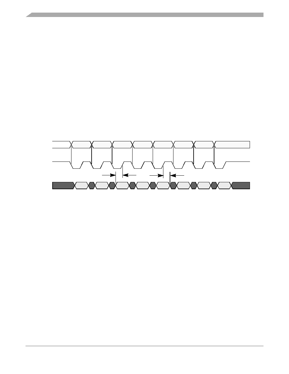
7.2.1 Serial Clock (SCK)
The state of the SCK output normally remains a logic 1 during idle periods between data transfers. The
first falling edge of SCK signals the beginning of a data transfer. At this time, the first bit of received data
may be presented at the SDI pin and the first bit of transmitted data is presented at the SDO pin (see
Figure 7-2). Data is captured at the SDI pin on the rising edge of SCK. The transfer is terminated upon
the eighth rising edge of SCK.
The master and slave modes of operation differ only by the sourcing of SCK. In master mode, SCK is
driven from an internal source within the MCU. In slave mode, SCK is driven from a source external to the
MCU. The SCK frequency is dependent upon the SPR0 and SPR1 bits located in the mask option
register. Refer to 11.2 Mask Option Register for a description of available SCK frequencies.
Figure 7-2. SIOP Timing Diagram
7.2.2 Serial Data Input (SDI)
The SDI pin becomes an input as soon as the SIOP subsystem is enabled. New data may be presented
to the SDI pin on the falling edge of SCK.However, valid data must be present at least 100 nanoseconds
before the rising edge of SCK and remain valid for 100 nanoseconds after the rising edge of SCK. See
7.2.3 Serial Data Output (SDO)
The SDO pin becomes an output as soon as the SIOP subsystem is enabled. Prior to enabling the SIOP,
PB5 can be initialized to determine the beginning state. While the SIOP is enabled, PB5 cannot be used
as a standard output since that pin is connected to the last stage of the SIOP serial shift register. Mask
option register bit LSBF permits data to be transmitted in either the MSB first format or the LSB first format.
Refer to 11.2 Mask Option Register for MOR LSBF programming information.
On the first falling edge of SCK, the first data bit will be shifted out to the SDO pin. The remaining data
bits will be shifted out to the SDO pin on subsequent falling edges of SCK. The SDO pin will present valid
data at least 100 nanoseconds before the rising edge of the SCK and remain valid for 100 nanoseconds
after the rising edge of SCK. See Figure 7-2.
SCK
SDO
SDI
100 ns
BIT 0
BIT 1
BIT 2
BIT 3
BIT 4
BIT 5
BIT 6
BIT 7
BIT 0
BIT 1
BIT 2
BIT 3
BIT 4
BIT 5
BIT 6
BIT 7
相关PDF资料 |
PDF描述 |
|---|---|
| HR25A-7J-4S | CONN JACK 4POS FEMALE SOLDER |
| PKG.M0.6SL.LG | CONN RCPT 6POS PNL MNT SKT SLDR |
| PKG.M0.4SL.LG | CONN RCPT 4POS PNL MNT SKT SLDR |
| AT85C51SND3B1-7FTUL | IC DECODER/ENCODER DGTL 100CBGA |
| JN1FS04FKK | CONN PLUG 4POS R/A W/SOCKET SLD |
相关代理商/技术参数 |
参数描述 |
|---|---|
| MC705SR3CFBE | 功能描述:8位微控制器 -MCU 8B MCU 192 BYTES RAM RoHS:否 制造商:Silicon Labs 核心:8051 处理器系列:C8051F39x 数据总线宽度:8 bit 最大时钟频率:50 MHz 程序存储器大小:16 KB 数据 RAM 大小:1 KB 片上 ADC:Yes 工作电源电压:1.8 V to 3.6 V 工作温度范围:- 40 C to + 105 C 封装 / 箱体:QFN-20 安装风格:SMD/SMT |
| MC705X32CFUE4 | 功能描述:IC MCU 8BIT 528RAM 64-QFP RoHS:是 类别:集成电路 (IC) >> 嵌入式 - 微控制器, 系列:HC05 标准包装:1 系列:87C 核心处理器:MCS 51 芯体尺寸:8-位 速度:16MHz 连通性:SIO 外围设备:- 输入/输出数:32 程序存储器容量:8KB(8K x 8) 程序存储器类型:OTP EEPROM 大小:- RAM 容量:256 x 8 电压 - 电源 (Vcc/Vdd):4 V ~ 6 V 数据转换器:- 振荡器型:外部 工作温度:0°C ~ 70°C 封装/外壳:44-DIP 包装:管件 其它名称:864285 |
| MC705X32CFUE4R | 功能描述:IC MCU 8BIT 32K FLASH 64-QFP RoHS:是 类别:集成电路 (IC) >> 嵌入式 - 微控制器, 系列:HC05 标准包装:1 系列:AVR® ATmega 核心处理器:AVR 芯体尺寸:8-位 速度:16MHz 连通性:I²C,SPI,UART/USART 外围设备:欠压检测/复位,POR,PWM,WDT 输入/输出数:32 程序存储器容量:32KB(16K x 16) 程序存储器类型:闪存 EEPROM 大小:1K x 8 RAM 容量:2K x 8 电压 - 电源 (Vcc/Vdd):2.7 V ~ 5.5 V 数据转换器:A/D 8x10b 振荡器型:内部 工作温度:-40°C ~ 125°C 封装/外壳:44-TQFP 包装:剪切带 (CT) 其它名称:ATMEGA324P-B15AZCT |
| MC705X32MFUE4 | 功能描述:IC MCU 8BIT 32K FLASH 64-QFP RoHS:是 类别:集成电路 (IC) >> 嵌入式 - 微控制器, 系列:HC05 标准包装:1 系列:AVR® ATmega 核心处理器:AVR 芯体尺寸:8-位 速度:16MHz 连通性:I²C,SPI,UART/USART 外围设备:欠压检测/复位,POR,PWM,WDT 输入/输出数:32 程序存储器容量:32KB(16K x 16) 程序存储器类型:闪存 EEPROM 大小:1K x 8 RAM 容量:2K x 8 电压 - 电源 (Vcc/Vdd):2.7 V ~ 5.5 V 数据转换器:A/D 8x10b 振荡器型:内部 工作温度:-40°C ~ 125°C 封装/外壳:44-TQFP 包装:剪切带 (CT) 其它名称:ATMEGA324P-B15AZCT |
| MC705X32MFUE4R | 功能描述:IC MCU 8BIT 32K FLASH 64-QFP RoHS:是 类别:集成电路 (IC) >> 嵌入式 - 微控制器, 系列:HC05 标准包装:1 系列:87C 核心处理器:MCS 51 芯体尺寸:8-位 速度:16MHz 连通性:SIO 外围设备:- 输入/输出数:32 程序存储器容量:8KB(8K x 8) 程序存储器类型:OTP EEPROM 大小:- RAM 容量:256 x 8 电压 - 电源 (Vcc/Vdd):4 V ~ 6 V 数据转换器:- 振荡器型:外部 工作温度:0°C ~ 70°C 封装/外壳:44-DIP 包装:管件 其它名称:864285 |
发布紧急采购,3分钟左右您将得到回复。