- 您现在的位置:买卖IC网 > PDF目录4041 > MC7457RX867NC (Freescale Semiconductor)IC MPU RISC 32BIT 483FCCBGA PDF资料下载
参数资料
| 型号: | MC7457RX867NC |
| 厂商: | Freescale Semiconductor |
| 文件页数: | 19/71页 |
| 文件大小: | 0K |
| 描述: | IC MPU RISC 32BIT 483FCCBGA |
| 标准包装: | 36 |
| 系列: | MPC74xx |
| 处理器类型: | 32-位 MPC74xx PowerPC |
| 速度: | 867MHz |
| 电压: | 1.1V |
| 安装类型: | 表面贴装 |
| 封装/外壳: | 483-BCBGA,FCCBGA |
| 供应商设备封装: | 483-FCCBGA(29x29) |
| 包装: | 托盘 |
第1页第2页第3页第4页第5页第6页第7页第8页第9页第10页第11页第12页第13页第14页第15页第16页第17页第18页当前第19页第20页第21页第22页第23页第24页第25页第26页第27页第28页第29页第30页第31页第32页第33页第34页第35页第36页第37页第38页第39页第40页第41页第42页第43页第44页第45页第46页第47页第48页第49页第50页第51页第52页第53页第54页第55页第56页第57页第58页第59页第60页第61页第62页第63页第64页第65页第66页第67页第68页第69页第70页第71页
MPC7457 RISC Microprocessor Hardware Specifications, Rev. 8
Electrical and Thermal Characteristics
Freescale Semiconductor
26
5.2.4.2
L3 Bus AC Specifications for DDR MSUG2 SRAMs
When using DDR MSUG2 SRAMs at the L3 interface, the parts should be connected as shown in Figure 9.
Outputs from the MPC7457 are actually launched on the edges of an internal clock phase-aligned to
SYSCLK (adjusted for core and L3 frequency divisors). L3_CLK0 and L3_CLK1 are this internal clock
output with 90° phase delay, so outputs are shown synchronous to L3_CLK0 and L3_CLK1. Output valid
times are typically negative when referenced to L3_CLKn because the data is launched one-quarter period
before L3_CLKn to provide adequate setup time at the SRAM after the delay-matched address, control,
data, and L3_CLKn signals have propagated across the printed-wiring board.
Inputs to the MPC7457 are source-synchronous with the CQ clock generated by the DDR MSUG2
SRAMs. These CQ clocks are received on the L3_ECHO_CLKn inputs of the MPC7457. An internal
circuit delays the incoming L3_ECHO_CLKn signal such that it is positioned within the valid data
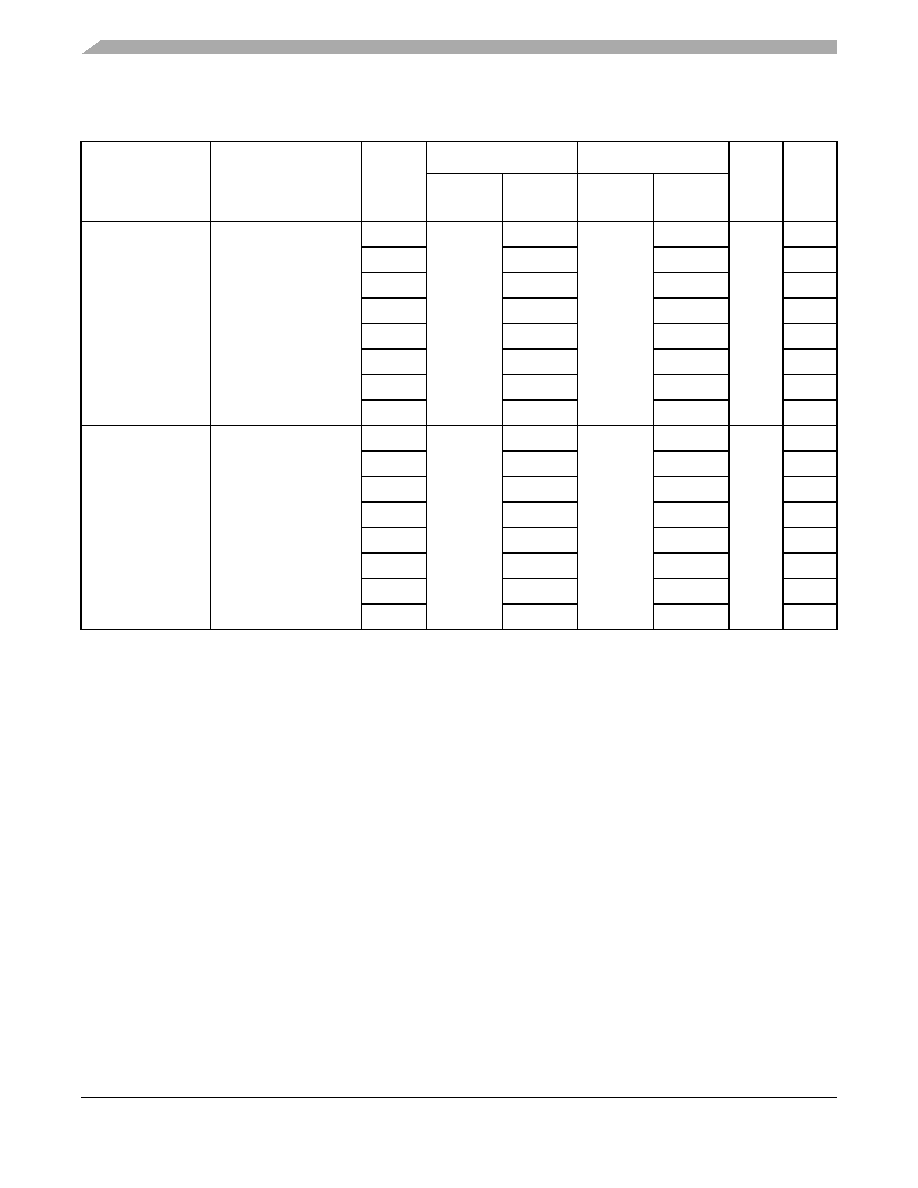
L3CLK
n_OH
All signals latched by
SRAM connected to
L3_CLK
n
0b000
tL3CHOV,
tL3CHDV,
tL3CLDV
0tL3CHOX,
tL3CHDX,
tL3CLDX
0ps
4
0b001
– 50
5
0b010
– 100
5
0b011
– 150
5
0b100
– 200
5
0b101
– 250
5
0b110
– 300
5
0b111
– 350
5
L3DOH
n
L3_DATA[
n:n+7],
L3_DP[
n/8]
0b000
tL3CHDV,
tL3CLDV
0tL3CHDX,
tL3CLDX
0ps
4
0b001
+ 50
0b010
+ 100
0b011
+ 150
0b100
+ 200
0b101
+ 250
0b111
+ 300
0b111
+ 350
Notes:
1. See the
MPC7450 RISC Microprocessor Family User’s Manual for specific information regarding L3OHCR.
3. Approximate delay verified by simulation; not tested or characterized.
4. Default value.
5. Increasing values of L3CLK
n_OH delay the L3_CLKn signal, effectively decreasing the output valid and output hold times of
all signals latched relative to that clock signal by the SRAM; see Figure 9 and Figure 11.
Table 12. Effect of L3OHCR Settings on L3 Bus AC Timing (continued)
At recommended operating conditions. See Table 4.
Field Name1
Affected Signals
Value
Output Valid Time
Output Hold Time
Unit
Notes
Parameter
Symbol 2
Change 3
Parameter
Symbol 2
Change 3
相关PDF资料 |
PDF描述 |
|---|---|
| FMC36DRAS | CONN EDGECARD 72POS R/A .100 SLD |
| MC68EC040RC40A | IC MPU 32BIT 40MHZ 179-PGA |
| MPC8560VTAQFC | MPU POWERQUICC III 783FCPBGA |
| MPC8548EVTATGB | MPU POWERQUICC III 783-PBGA |
| MPC8548EPXATGB | MPU POWERQUICC III 783-PBGA |
相关代理商/技术参数 |
参数描述 |
|---|---|
| MC7457TRX1000LC | 制造商:Freescale Semiconductor 功能描述:MPC74XX RISC 32-BIT 0.13UM 1GHZ 1.5V/1.8V/2.5V 483-PIN FCCBG - Trays |
| MC7457TRX1000NC | 功能描述:微处理器 - MPU APOLO7 RV1.2 1.1V -40C RoHS:否 制造商:Atmel 处理器系列:SAMA5D31 核心:ARM Cortex A5 数据总线宽度:32 bit 最大时钟频率:536 MHz 程序存储器大小:32 KB 数据 RAM 大小:128 KB 接口类型:CAN, Ethernet, LIN, SPI,TWI, UART, USB 工作电源电压:1.8 V to 3.3 V 最大工作温度:+ 85 C 安装风格:SMD/SMT 封装 / 箱体:FBGA-324 |
| MC7457TRX1267LC | 制造商:Freescale Semiconductor 功能描述:MPC74XX RISC 32-BIT 0.13UM 1.267GHZ 1.5V/1.8V/2.5V 483-PIN F - Trays |
| MC7457VG1000LC | 功能描述:微处理器 - MPU APOLO7 RV1.2 1.3V 105C RoHS:否 制造商:Atmel 处理器系列:SAMA5D31 核心:ARM Cortex A5 数据总线宽度:32 bit 最大时钟频率:536 MHz 程序存储器大小:32 KB 数据 RAM 大小:128 KB 接口类型:CAN, Ethernet, LIN, SPI,TWI, UART, USB 工作电源电压:1.8 V to 3.3 V 最大工作温度:+ 85 C 安装风格:SMD/SMT 封装 / 箱体:FBGA-324 |
| MC7457VG1000NC | 功能描述:微处理器 - MPU APOLO7 RV1.2 1.1V 105C RoHS:否 制造商:Atmel 处理器系列:SAMA5D31 核心:ARM Cortex A5 数据总线宽度:32 bit 最大时钟频率:536 MHz 程序存储器大小:32 KB 数据 RAM 大小:128 KB 接口类型:CAN, Ethernet, LIN, SPI,TWI, UART, USB 工作电源电压:1.8 V to 3.3 V 最大工作温度:+ 85 C 安装风格:SMD/SMT 封装 / 箱体:FBGA-324 |
发布紧急采购,3分钟左右您将得到回复。