- 您现在的位置:买卖IC网 > PDF目录4037 > MC7457VG1000LC (Freescale Semiconductor)IC MPU RISC 1000MHZ 483FCCBGA PDF资料下载
参数资料
| 型号: | MC7457VG1000LC |
| 厂商: | Freescale Semiconductor |
| 文件页数: | 24/71页 |
| 文件大小: | 0K |
| 描述: | IC MPU RISC 1000MHZ 483FCCBGA |
| 标准包装: | 36 |
| 系列: | MPC74xx |
| 处理器类型: | 32-位 MPC74xx PowerPC |
| 速度: | 1.0GHz |
| 电压: | 1.3V |
| 安装类型: | 表面贴装 |
| 封装/外壳: | 483-BCBGA,FCCBGA |
| 供应商设备封装: | 483-FCCBGA(29x29) |
| 包装: | 托盘 |
第1页第2页第3页第4页第5页第6页第7页第8页第9页第10页第11页第12页第13页第14页第15页第16页第17页第18页第19页第20页第21页第22页第23页当前第24页第25页第26页第27页第28页第29页第30页第31页第32页第33页第34页第35页第36页第37页第38页第39页第40页第41页第42页第43页第44页第45页第46页第47页第48页第49页第50页第51页第52页第53页第54页第55页第56页第57页第58页第59页第60页第61页第62页第63页第64页第65页第66页第67页第68页第69页第70页第71页
MPC7457 RISC Microprocessor Hardware Specifications, Rev. 8
Electrical and Thermal Characteristics
Freescale Semiconductor
30
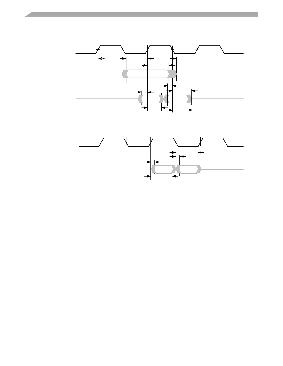
Figure 10 shows the L3 bus timing diagrams for the MPC7457 interfaced to MSUG2 SRAMs.
Figure 10. L3 Bus Timing Diagrams for L3 Cache DDR SRAMs
5.2.4.3
L3 Bus AC Specifications for PB2 and Late Write SRAMs
When using PB2 or Late Write SRAMs at the L3 interface, the parts should be connected as shown in
Figure 11. These SRAMs are synchronous to the MPC7457; one L3_CLKn signal is output to each SRAM
to latch address, control, and write data. Read data is launched by the SRAM synchronous to the delayed
L3_CLKn signal it received. The MPC7457 needs a copy of that delayed clock which launched the SRAM
read data to know when the returning data will be valid. Therefore, L3_ECHO_CLK1 and
L3_ECHO_CLK3 must be routed halfway to the SRAMs and returned to the MPC7457 inputs
L3_ECHO_CLK0 and L3_ECHO_CLK2, respectively. Thus, L3_ECHO_CLK0 and L3_ECHO_CLK2
are phase-aligned with the input clock received at the SRAMs. The MPC7457 will latch the incoming data
on the rising edge of L3_ECHO_CLK0 and L3_ECHO_CLK2.
Table 14 provides the L3 bus interface AC timing specifications for the configuration shown in Figure 11,
L3_ECHO_CLK[0,1,2,3]
L3 Data and Data
VM
VM = Midpoint Voltage (GVDD/2)
Parity Inputs
L3_CLK[0,1]
ADDR, L3CNTL
VM
tL3CHOV
tL3CHOX
VM
L3DATA WRITE
tL3CHOZ
VM
tL3CHDV
tL3CHDX
VM
Outputs
Inputs
tL3CLDV
tL3CLDX
tL3CLDZ
tL3DVEH
tL3DXEL
tL3DVEL
tL3DXEH
Note: t
L3DVEH and tL3DVEL as drawn here are negative numbers, that is, input setup time is
time after the clock edge.
Note: t
L3CHDV and tL3CLDV as drawn here will be negative numbers, that is, output valid time will be
time before the clock edge.
相关PDF资料 |
PDF描述 |
|---|---|
| MC68040RC33V | IC MICROPROCESSOR 32BIT 182-PGA |
| FH40-10S-0.5SV | CONN FPC/FFC 10POS .5MM VERT SMD |
| MC68LC040RC40A | IC MPU 32BIT 40MHZ 179-PGA |
| XPC8260CZUIHBC | IC MPU POWERQUICC II 480-TBGA |
| XPC8260CVVIHBC | IC MPU POWERQUICC II 480-TBGA |
相关代理商/技术参数 |
参数描述 |
|---|---|
| MC7457VG1000NC | 功能描述:微处理器 - MPU APOLO7 RV1.2 1.1V 105C RoHS:否 制造商:Atmel 处理器系列:SAMA5D31 核心:ARM Cortex A5 数据总线宽度:32 bit 最大时钟频率:536 MHz 程序存储器大小:32 KB 数据 RAM 大小:128 KB 接口类型:CAN, Ethernet, LIN, SPI,TWI, UART, USB 工作电源电压:1.8 V to 3.3 V 最大工作温度:+ 85 C 安装风格:SMD/SMT 封装 / 箱体:FBGA-324 |
| MC7457VG1267LC | 功能描述:微处理器 - MPU APOLO7 RV1.2 1.3V 105C RoHS:否 制造商:Atmel 处理器系列:SAMA5D31 核心:ARM Cortex A5 数据总线宽度:32 bit 最大时钟频率:536 MHz 程序存储器大小:32 KB 数据 RAM 大小:128 KB 接口类型:CAN, Ethernet, LIN, SPI,TWI, UART, USB 工作电源电压:1.8 V to 3.3 V 最大工作温度:+ 85 C 安装风格:SMD/SMT 封装 / 箱体:FBGA-324 |
| MC7457VG733NC | 功能描述:IC MPU RISC 733MHZ 483FCCBGA RoHS:是 类别:集成电路 (IC) >> 嵌入式 - 微处理器 系列:MPC74xx 标准包装:1 系列:MPC85xx 处理器类型:32-位 MPC85xx PowerQUICC III 特点:- 速度:1.2GHz 电压:1.1V 安装类型:表面贴装 封装/外壳:783-BBGA,FCBGA 供应商设备封装:783-FCPBGA(29x29) 包装:托盘 |
| MC7457VG867NC | 功能描述:微处理器 - MPU APOLO7 RV1.2 1.1V 105C RoHS:否 制造商:Atmel 处理器系列:SAMA5D31 核心:ARM Cortex A5 数据总线宽度:32 bit 最大时钟频率:536 MHz 程序存储器大小:32 KB 数据 RAM 大小:128 KB 接口类型:CAN, Ethernet, LIN, SPI,TWI, UART, USB 工作电源电压:1.8 V to 3.3 V 最大工作温度:+ 85 C 安装风格:SMD/SMT 封装 / 箱体:FBGA-324 |
| MC74A5-33SNTR | 制造商:Rochester Electronics LLC 功能描述:- Tape and Reel |
发布紧急采购,3分钟左右您将得到回复。