- 您现在的位置:买卖IC网 > PDF目录25621 > MC74AC04DR2 (MOTOROLA INC) AC SERIES, HEX 1-INPUT INVERT GATE, PDSO14 PDF资料下载
参数资料
| 型号: | MC74AC04DR2 |
| 厂商: | MOTOROLA INC |
| 元件分类: | 门电路 |
| 英文描述: | AC SERIES, HEX 1-INPUT INVERT GATE, PDSO14 |
| 封装: | PLASTIC, SOIC-14 |
| 文件页数: | 2/5页 |
| 文件大小: | 123K |
| 代理商: | MC74AC04DR2 |
MC74AC04 MC74ACT04
5-2
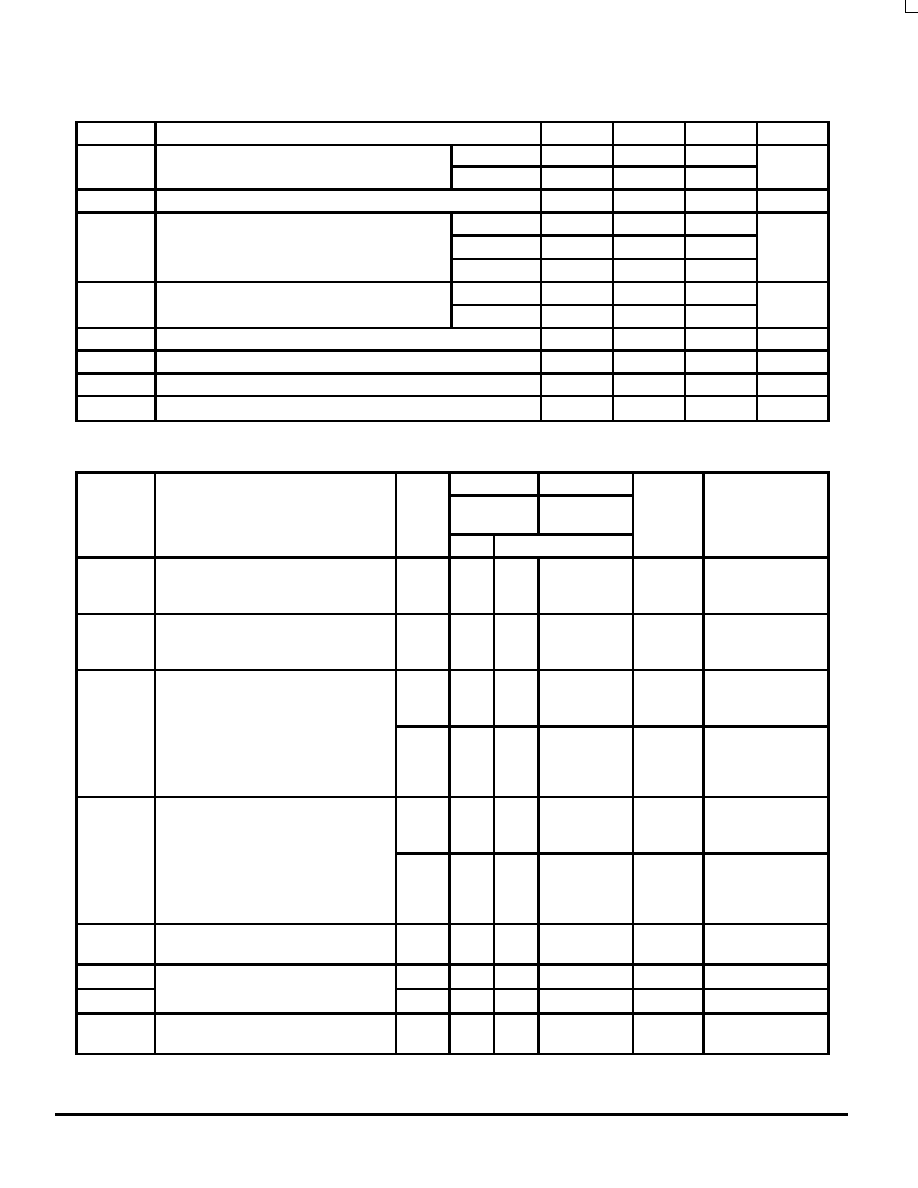
FACT DATA
RECOMMENDED OPERATING CONDITIONS
Symbol
Parameter
Min
Typ
Max
Unit
VCC
Supply Voltage
′AC
2.0
5.0
6.0
V
VCC
Supply Voltage
′ACT
4.5
5.0
5.5
V
Vin, Vout
DC Input Voltage, Output Voltage (Ref. to GND)
0
VCC
V
tr, tf
Input Rise and Fall Time (Note 1)
′AC Devices except Schmitt Inputs
VCC @ 3.0 V
150
tr, tf
Input Rise and Fall Time (Note 1)
′AC Devices except Schmitt Inputs
VCC @ 4.5 V
40
ns/V
r, tf
′AC Devices except Schmitt Inputs
VCC @ 5.5 V
25
tr, tf
Input Rise and Fall Time (Note 2)
′ACT Devices except Schmitt Inputs
VCC @ 4.5 V
10
ns/V
tr, tf
Input Rise and Fall Time (Note 2)
′ACT Devices except Schmitt Inputs
VCC @ 5.5 V
8.0
ns/V
TJ
Junction Temperature (PDIP)
140
°C
TA
Operating Ambient Temperature Range
–40
25
85
°C
IOH
Output Current — High
–24
mA
IOL
Output Current — Low
24
mA
1. Vin from 30% to 70% VCC; see individual Data Sheets for devices that differ from the typical input rise and fall times.
2. Vin from 0.8 V to 2.0 V; see individual Data Sheets for devices that differ from the typical input rise and fall times.
DC CHARACTERISTICS
Symbol
Parameter
VCC
(V)
74AC
Unit
Conditions
Symbol
Parameter
VCC
(V)
TA = +25°C
TA =
–40
°C to +85°C
Unit
Conditions
Typ
Guaranteed Limits
VIH
Minimum High Level
Input Voltage
3.0
1.5
2.1
VOUT = 0.1 V
Input Voltage
4.5
2.25
3.15
V
or VCC – 0.1 V
5.5
2.75
3.85
VIL
Maximum Low Level
Input Voltage
3.0
1.5
0.9
VOUT = 0.1 V
Input Voltage
4.5
2.25
1.35
V
or VCC – 0.1 V
5.5
2.75
1.65
VOH
Minimum High Level
Output Voltage
3.0
2.99
2.9
IOUT = –50 A
Output Voltage
4.5
4.49
4.4
V
5.5
5.49
5.4
V
*VIN = VIL or VIH
3.0
2.56
2.46
V
–12 mA
4.5
3.86
3.76
V
IOH
–24 mA
5.5
4.86
4.76
–24 mA
VOL
Maximum Low Level
Output Voltage
3.0
0.002
0.1
IOUT = 50 A
Output Voltage
4.5
0.001
0.1
V
5.5
0.001
0.1
V
*VIN = VIL or VIH
3.0
0.36
0.44
V
12 mA
4.5
0.36
0.44
V
IOL
24 mA
5.5
0.36
0.44
24 mA
IIN
Maximum Input
Leakage Current
5.5
±0.1
±1.0
A
VI = VCC, GND
Leakage Current
5.5
±0.1
±1.0
A
VI = VCC, GND
IOLD
Minimum Dynamic
Output Current
5.5
75
mA
VOLD = 1.65 V Max
IOHD
Output Current
5.5
–75
mA
VOHD = 3.85 V Min
ICC
Maximum Quiescent
Supply Current
5.5
4.0
40
A
VIN = VCC or GND
Supply Current
5.5
4.0
40
A
VIN = VCC or GND
* All outputs loaded; thresholds on input associated with output under test.
Maximum test duration 2.0 ms, one output loaded at a time.
Note: IIN and ICC @ 3.0 V are guaranteed to be less than or equal to the respective limit @ 5.5 V VCC.
相关PDF资料 |
PDF描述 |
|---|---|
| MC74AC132DR2 | AC SERIES, QUAD 2-INPUT NAND GATE, PDSO14 |
| MC74AC132DT | AC SERIES, QUAD 2-INPUT NAND GATE, PDSO14 |
| MC74AC244MR2 | AC SERIES, DUAL 4-BIT DRIVER, TRUE OUTPUT, PDSO20 |
| MC74AC563DWR2 | AC SERIES, 8-BIT DRIVER, INVERTED OUTPUT, PDSO20 |
| MC74AC564DW | AC SERIES, 8-BIT DRIVER, INVERTED OUTPUT, PDSO20 |
相关代理商/技术参数 |
参数描述 |
|---|---|
| MC74AC04DR2G | 功能描述:变换器 2-6V CMOS Hex RoHS:否 制造商:NXP Semiconductors 电路数量:6 逻辑系列:74ABT 逻辑类型:BiCMOS 高电平输出电流:- 15 mA 低电平输出电流:20 mA 传播延迟时间:2.2 ns 电源电压-最大:5.5 V 电源电压-最小:4.5 V 最大工作温度:+ 85 C 最小工作温度:- 40 C 工作温度范围: 封装 / 箱体:DIP-14 封装:Tube |
| MC74AC04DT | 制造商:ONSEMI 制造商全称:ON Semiconductor 功能描述:Hex Inverter |
| MC74AC04DTR2 | 功能描述:变换器 2-6V CMOS Hex RoHS:否 制造商:NXP Semiconductors 电路数量:6 逻辑系列:74ABT 逻辑类型:BiCMOS 高电平输出电流:- 15 mA 低电平输出电流:20 mA 传播延迟时间:2.2 ns 电源电压-最大:5.5 V 电源电压-最小:4.5 V 最大工作温度:+ 85 C 最小工作温度:- 40 C 工作温度范围: 封装 / 箱体:DIP-14 封装:Tube |
| MC74AC04DTR2G | 功能描述:变换器 2-6V CMOS Hex RoHS:否 制造商:NXP Semiconductors 电路数量:6 逻辑系列:74ABT 逻辑类型:BiCMOS 高电平输出电流:- 15 mA 低电平输出电流:20 mA 传播延迟时间:2.2 ns 电源电压-最大:5.5 V 电源电压-最小:4.5 V 最大工作温度:+ 85 C 最小工作温度:- 40 C 工作温度范围: 封装 / 箱体:DIP-14 封装:Tube |
| MC74AC04M | 制造商:Rochester Electronics LLC 功能描述:- Bulk |
发布紧急采购,3分钟左右您将得到回复。