- 您现在的位置:买卖IC网 > PDF目录29124 > MC74AC323DW (ON SEMICONDUCTOR) AC SERIES, 8-BIT BIDIRECTIONAL PARALLEL IN PARALLEL OUT SHIFT REGISTER, TRUE OUTPUT, PDSO20 PDF资料下载
参数资料
| 型号: | MC74AC323DW |
| 厂商: | ON SEMICONDUCTOR |
| 元件分类: | 计数移位寄存器 |
| 英文描述: | AC SERIES, 8-BIT BIDIRECTIONAL PARALLEL IN PARALLEL OUT SHIFT REGISTER, TRUE OUTPUT, PDSO20 |
| 封装: | PLASTIC, SOIC-20 |
| 文件页数: | 6/12页 |
| 文件大小: | 98K |
| 代理商: | MC74AC323DW |
MC74AC323 MC74ACT323
http://onsemi.com
3
FUNCTIONAL DESCRIPTION
The MC74AC323/74ACT323 contains eight edge-
triggered D-type flip-flops and the interstage logic
necessary to perform synchronous reset, shift left, shift
right, parallel load and hold operations. The type of
operation is determined by S0 and S1 as shown in the Mode
Select Table. All flip-flop outputs are brought out through
3 state buffers to separate I/O pins that also serve as data
inputs in the parallel load mode. Q0 and Q7 are also brought
out on other pins for expansion in serial shifting of longer
words.
A LOW signal on SR overrides the Select inputs and
allows the flip-flops to be reset by the next rising edge of
CP. All other state changes are also initiated by the
LOW-to-HIGH CP transition. Inputs can change when the
clock is in either state provided only that the recommended
setup and hold times, relative to the rising edge of CP, are
observed.
A HIGH signal on either OE1 or OE2 disables the 3-state
buffers and puts the I/O pins in the high impedance state.
In this condition the shift, hold, load and reset operations
can still occur. The 3-state buffers are also disabled by
HIGH signals on both S0 and S1 in preparation for a parallel
load operation.
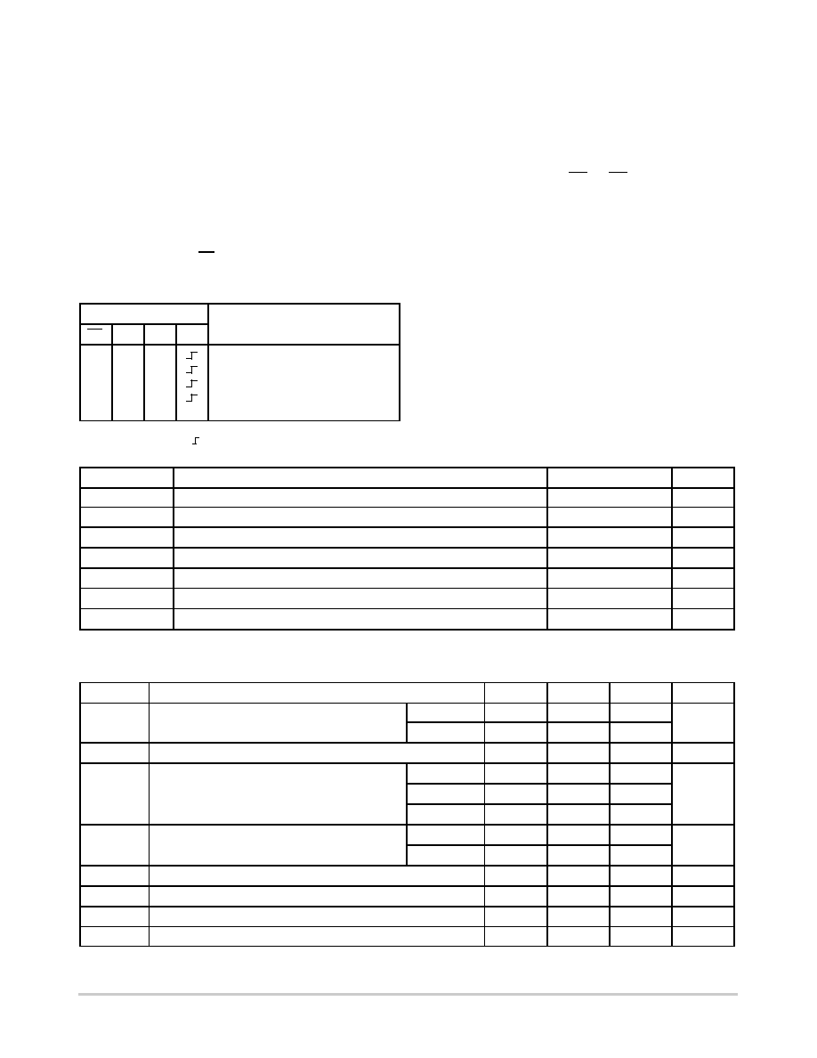
TRUTH TABLE
Inputs
Response
SR
S1
S0
CP
Response
L
X
Synchronous Reset; Q0 – Q7 = LOW
H
Parallel Load; I/On → Qn
H
L
H
Shift Right; DS0 → Q0, Q0 → Q1, etc.
H
L
Shift Left; DS7 → Q7, Q7 → Q6, etc.
H
L
X
Hold
H = HIGH Voltage Level
L = LOW Voltage Level
X = Immaterial
= LOW-to-HIGH Clock Transition
MAXIMUM RATINGS*
Symbol
Parameter
Value
Unit
VCC
DC Supply Voltage (Referenced to GND)
–0.5 to +7.0
V
Vin
DC Input Voltage (Referenced to GND)
–0.5 to VCC +0.5
V
Vout
DC Output Voltage (Referenced to GND)
–0.5 to VCC +0.5
V
Iin
DC Input Current, per Pin
±20
mA
Iout
DC Output Sink/Source Current, per Pin
±50
mA
ICC
DC VCC or GND Current per Output Pin
±50
mA
Tstg
Storage Temperature
–65 to +150
°C
* Maximum Ratings are those values beyond which damage to the device may occur. Functional operation should be restricted to the Recommended
Operating Conditions.
RECOMMENDED OPERATING CONDITIONS
Symbol
Parameter
Min
Typ
Max
Unit
V
Supply Voltage
′AC
2.0
5.0
6.0
V
VCC
Supply Voltage
′ACT
4.5
5.0
5.5
V
Vin, Vout
DC Input Voltage, Output Voltage (Ref. to GND)
0
VCC
V
VCC @ 3.0 V
150
tr, tf
Input Rise and Fall Time (Note 1)
′AC Devices except Schmitt Inputs
VCC @ 4.5 V
40
ns/V
r, f
′AC Devices except Schmitt Inputs
VCC @ 5.5 V
25
t t
Input Rise and Fall Time (Note 2)
VCC @ 4.5 V
10
ns/V
tr, tf
In ut Rise and Fall Time (Note 2)
′ACT Devices except Schmitt Inputs
VCC @ 5.5 V
8.0
ns/V
TJ
Junction Temperature (PDIP)
140
°C
TA
Operating Ambient Temperature Range
–40
25
85
°C
IOH
Output Current — High
–24
mA
IOL
Output Current — Low
24
mA
1. Vin from 30% to 70% VCC; see individual Data Sheets for devices that differ from the typical input rise and fall times.
2. Vin from 0.8 V to 2.0 V; see individual Data Sheets for devices that differ from the typical input rise and fall times.
相关PDF资料 |
PDF描述 |
|---|---|
| MC74AC323DWR2 | AC SERIES, 8-BIT BIDIRECTIONAL PARALLEL IN PARALLEL OUT SHIFT REGISTER, TRUE OUTPUT, PDSO20 |
| MC74AC4020DCR2 | AC SERIES, ASYN NEGATIVE EDGE TRIGGERED 14-BIT UP BINARY COUNTER, PDSO16 |
| MC74AC568DWCR2 | AC SERIES, SYN POSITIVE EDGE TRIGGERED 4-BIT BIDIRECTIONAL DECADE COUNTER, PDSO20 |
| MC74AC640NC | AC SERIES, 8-BIT TRANSCEIVER, INVERTED OUTPUT, PDIP20 |
| MC74ACT640NC | ACT SERIES, 8-BIT TRANSCEIVER, INVERTED OUTPUT, PDIP20 |
相关代理商/技术参数 |
参数描述 |
|---|---|
| MC74AC323N | 制造商:MOTOROLA 制造商全称:Motorola, Inc 功能描述:8-INPUT UNIVERSAL SHIFT/ STORAGE REGISTER WITH SYNCHRONOUS RESET AND COMMON I/O PINS |
| MC74AC32D | 功能描述:逻辑门 2-6V Quad 2-Input RoHS:否 制造商:Texas Instruments 产品:OR 逻辑系列:LVC 栅极数量:2 线路数量(输入/输出):2 / 1 高电平输出电流:- 16 mA 低电平输出电流:16 mA 传播延迟时间:3.8 ns 电源电压-最大:5.5 V 电源电压-最小:1.65 V 最大工作温度:+ 125 C 安装风格:SMD/SMT 封装 / 箱体:DCU-8 封装:Reel |
| MC74AC32-D | 制造商:ONSEMI 制造商全称:ON Semiconductor 功能描述:QUAD 2-INPUT OR GATE |
| MC74AC32DG | 功能描述:逻辑门 2-6V Quad 2-Input OR RoHS:否 制造商:Texas Instruments 产品:OR 逻辑系列:LVC 栅极数量:2 线路数量(输入/输出):2 / 1 高电平输出电流:- 16 mA 低电平输出电流:16 mA 传播延迟时间:3.8 ns 电源电压-最大:5.5 V 电源电压-最小:1.65 V 最大工作温度:+ 125 C 安装风格:SMD/SMT 封装 / 箱体:DCU-8 封装:Reel |
| MC74AC32DR2 | 功能描述:逻辑门 2-6V Quad 2-Input RoHS:否 制造商:Texas Instruments 产品:OR 逻辑系列:LVC 栅极数量:2 线路数量(输入/输出):2 / 1 高电平输出电流:- 16 mA 低电平输出电流:16 mA 传播延迟时间:3.8 ns 电源电压-最大:5.5 V 电源电压-最小:1.65 V 最大工作温度:+ 125 C 安装风格:SMD/SMT 封装 / 箱体:DCU-8 封装:Reel |
发布紧急采购,3分钟左右您将得到回复。