参数资料
| 型号: | MC74AC374DTR2 |
| 厂商: | ON Semiconductor |
| 文件页数: | 3/10页 |
| 文件大小: | 0K |
| 描述: | IC FLIP FLOP OCT D 3ST 20-TSSOP |
| 产品变化通告: | Product Obsolescence 24/Jan/2011 |
| 标准包装: | 2,500 |
| 系列: | 74AC |
| 功能: | 标准 |
| 类型: | D 型总线 |
| 输出类型: | 三态非反相 |
| 元件数: | 1 |
| 每个元件的位元数: | 8 |
| 频率 - 时钟: | 155MHz |
| 延迟时间 - 传输: | 8ns |
| 触发器类型: | 正边沿 |
| 输出电流高,低: | 24mA,24mA |
| 电源电压: | 2 V ~ 6 V |
| 工作温度: | -40°C ~ 85°C |
| 安装类型: | 表面贴装 |
| 封装/外壳: | 20-TSSOP(0.173",4.40mm 宽) |
| 包装: | 带卷 (TR) |
MC74AC374, MC74ACT374
http://onsemi.com
2
TRUTH TABLE
Inputs
Outputs
Dn
CP
OE
On
H
L
H
L
X
H
Z
H = HIGH Voltage Level
L = LOW Voltage Level
X = Immaterial
Z = High Impedance
= LOW-to-HIGH Transition
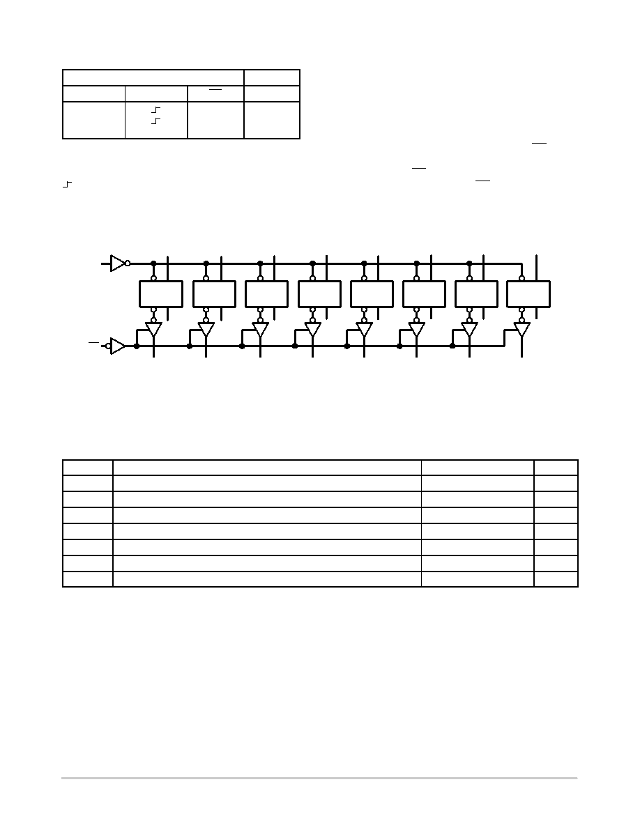
FUNCTIONAL DESCRIPTION
The MC74AC374/74ACT374 consists of eight edge
triggered flipflops with individual Dtype inputs and
3state true outputs. The buffered clock and buffered Output
Enable are common to all flipflops. The eight flipflops
will store the state of their individual D inputs that meet the
setup and hold time requirements on the LOWtoHIGH
Clock (CP) transition. With the Output Enable (OE) LOW,
the contents of the eight flipflops are available at the
outputs. When the OE is HIGH, the outputs go to the high
impedance state. Operation of the OE input does not affect
the state of the flipflops.
Figure 3. Logic Diagram
CP D
QQ
CP D
QQ
CP D
QQ
CP D
QQ
CP D
QQ
CP D
QQ
CP D
QQ
CP D
QQ
D0
D1
D2
D3
D4
D5
D6
D7
O0
O1
O2
O3
O4
O5
O6
O7
OE
CP
NOTE:
That this diagram is provided only for the understanding of logic
operations and should not be used to estimate propagation delays.
MAXIMUM RATINGS
Symbol
Parameter
Value
Unit
VCC
DC Supply Voltage (Referenced to GND)
0.5 to +7.0
V
VIN
DC Input Voltage (Referenced to GND)
0.5 to VCC +0.5
V
VOUT
DC Output Voltage (Referenced to GND)
0.5 to VCC +0.5
V
IIN
DC Input Current, per Pin
±20
mA
IOUT
DC Output Sink/Source Current, per Pin
±50
mA
ICC
DC VCC or GND Current per Output Pin
±50
mA
Tstg
Storage Temperature
65 to +150
°C
Stresses exceeding Maximum Ratings may damage the device. Maximum Ratings are stress ratings only. Functional operation above the
Recommended Operating Conditions is not implied. Extended exposure to stresses above the Recommended Operating Conditions may affect
device reliability.
相关PDF资料 |
PDF描述 |
|---|---|
| MC74AC273MELG | IC FLIP FLOP OCTAL D 20-SOEIAJ |
| MC74AC273DW | IC FLIP FLOP OCTAL D 20-SOIC |
| MC74AC273DTR2 | IC FLIP FLOP OCTAL D 20-TSSOP |
| VI-23R-MV-B1 | CONVERTER MOD DC/DC 7.5V 150W |
| MS3450W32-6AZ | CONN HSG RCPT 23POS WALLMNT PINS |
相关代理商/技术参数 |
参数描述 |
|---|---|
| MC74AC374DTR2G | 功能描述:触发器 2-6V CMOS Octal D-Type 3 State Out RoHS:否 制造商:Texas Instruments 电路数量:2 逻辑系列:SN74 逻辑类型:D-Type Flip-Flop 极性:Inverting, Non-Inverting 输入类型:CMOS 输出类型: 传播延迟时间:4.4 ns 高电平输出电流:- 16 mA 低电平输出电流:16 mA 电源电压-最大:5.5 V 最大工作温度:+ 85 C 安装风格:SMD/SMT 封装 / 箱体:X2SON-8 封装:Reel |
| MC74AC374DW | 功能描述:触发器 2-6V CMOS Octal RoHS:否 制造商:Texas Instruments 电路数量:2 逻辑系列:SN74 逻辑类型:D-Type Flip-Flop 极性:Inverting, Non-Inverting 输入类型:CMOS 输出类型: 传播延迟时间:4.4 ns 高电平输出电流:- 16 mA 低电平输出电流:16 mA 电源电压-最大:5.5 V 最大工作温度:+ 85 C 安装风格:SMD/SMT 封装 / 箱体:X2SON-8 封装:Reel |
| MC74AC374DWG | 功能描述:触发器 2-6V CMOS Octal D-Type 3 State Out RoHS:否 制造商:Texas Instruments 电路数量:2 逻辑系列:SN74 逻辑类型:D-Type Flip-Flop 极性:Inverting, Non-Inverting 输入类型:CMOS 输出类型: 传播延迟时间:4.4 ns 高电平输出电流:- 16 mA 低电平输出电流:16 mA 电源电压-最大:5.5 V 最大工作温度:+ 85 C 安装风格:SMD/SMT 封装 / 箱体:X2SON-8 封装:Reel |
| MC74AC374DWR2 | 功能描述:触发器 2-6V CMOS Octal RoHS:否 制造商:Texas Instruments 电路数量:2 逻辑系列:SN74 逻辑类型:D-Type Flip-Flop 极性:Inverting, Non-Inverting 输入类型:CMOS 输出类型: 传播延迟时间:4.4 ns 高电平输出电流:- 16 mA 低电平输出电流:16 mA 电源电压-最大:5.5 V 最大工作温度:+ 85 C 安装风格:SMD/SMT 封装 / 箱体:X2SON-8 封装:Reel |
| MC74AC374DWR2G | 功能描述:触发器 2-6V CMOS Octal D-Type 3 State Out RoHS:否 制造商:Texas Instruments 电路数量:2 逻辑系列:SN74 逻辑类型:D-Type Flip-Flop 极性:Inverting, Non-Inverting 输入类型:CMOS 输出类型: 传播延迟时间:4.4 ns 高电平输出电流:- 16 mA 低电平输出电流:16 mA 电源电压-最大:5.5 V 最大工作温度:+ 85 C 安装风格:SMD/SMT 封装 / 箱体:X2SON-8 封装:Reel |
发布紧急采购,3分钟左右您将得到回复。