- 您现在的位置:买卖IC网 > PDF目录2095 > MC74HC10ADTR2G (ON Semiconductor)IC GATE NAND TRIPLE 3INP 14TSSOP PDF资料下载
参数资料
| 型号: | MC74HC10ADTR2G |
| 厂商: | ON Semiconductor |
| 文件页数: | 2/6页 |
| 文件大小: | 0K |
| 描述: | IC GATE NAND TRIPLE 3INP 14TSSOP |
| 标准包装: | 2,500 |
| 系列: | 74HC |
| 逻辑类型: | 与非门 |
| 电路数: | 3 |
| 输入数: | 3 |
| 电源电压: | 2 V ~ 6 V |
| 电流 - 静态(最大值): | 1µA |
| 输出电流高,低: | 5.2mA,5.2mA |
| 逻辑电平 - 低: | 0.5 V ~ 1.8 V |
| 逻辑电平 - 高: | 1.5 V ~ 4.2 V |
| 额定电压和最大 CL 时的最大传播延迟: | 16ns @ 6V,50pF |
| 工作温度: | -55°C ~ 125°C |
| 安装类型: | 表面贴装 |
| 供应商设备封装: | 14-TSSOP |
| 封装/外壳: | 14-TSSOP(0.173",4.40mm 宽) |
| 包装: | 带卷 (TR) |
MC74HC10A
http://onsemi.com
2
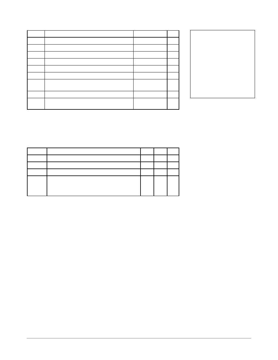
MAXIMUM RATINGS*
Symbol
Parameter
Value
Unit
VCC
DC Supply Voltage (Referenced to GND)
– 0.5 to + 7.0
V
Vin
DC Input Voltage (Referenced to GND)
– 0.5 to VCC + 0.5
V
Vout
DC Output Voltage (Referenced to GND)
– 0.5 to VCC + 0.5
V
Iin
DC Input Current, per Pin
± 20
mA
Iout
DC Output Current, per Pin
± 25
mA
ICC
DC Supply Current, VCC and GND Pins
± 50
mA
PD
Power Dissipation in Still Air
SOIC Package
TSSOP Package
500
450
mW
Tstg
Storage Temperature
– 65 to + 150
_C
TL
Lead Temperature, 1 mm from Case for 10 Seconds
(SOIC or TSSOP Package)
260
_C
Stresses exceeding Maximum Ratings may damage the device. Maximum Ratings are stress
ratings only. Functional operation above the Recommended Operating Conditions is not implied.
Extended exposure to stresses above the Recommended Operating Conditions may affect device
reliability.
Derating — SOIC Package: –7 mW/_C from 65_ to 125_C
TSSOP Package: 6.1 mW/_C from 65_ to 125_C
RECOMMENDED OPERATING CONDITIONS
Symbol
Parameter
Min
Max
Unit
VCC
DC Supply Voltage (Referenced to GND)
2.0
6.0
V
Vin, Vout
DC Input Voltage, Output Voltage (Referenced to GND)
0
VCC
V
TA
Operating Temperature, All Package Types
– 55
+ 125
_C
tr, tf
Input Rise and Fall Time
VCC = 2.0 V
(Figure 1)
VCC = 3.0 V
VCC = 4.5 V
VCC = 6.0 V
0
1000
600
500
400
ns
This device contains protection
circuitry to guard against damage
due to high static voltages or electric
fields. However, precautions must
be taken to avoid applications of any
voltage higher than maximum rated
voltages to this highimpedance cir-
cuit. For proper operation, Vin and
Vout should be constrained to the
range GND v (Vin or Vout) v VCC.
Unused inputs must always be
tied to an appropriate logic voltage
level (e.g., either GND or VCC).
Unused outputs must be left open.
相关PDF资料 |
PDF描述 |
|---|---|
| MC74HC11ADR2G | IC AND GATE 3INPUT 14 SOIC |
| MC74HC132AFELG | IC GATE NAND QUAD 2INP 14-SOEIAJ |
| MC74HC151ADG | IC DATA SELECT/MUX 8x1 16SOIC |
| MC74HC153ADG | IC DATA SELECT/MUX DL 4X1 16SOIC |
| MC74HC164ADTR2 | IC SHIFT REGISTER 8BIT 14-TSSOP |
相关代理商/技术参数 |
参数描述 |
|---|---|
| MC74HC10DR2 | 制造商:ON Semiconductor 功能描述:NAND Gate 3-Element 3-IN CMOS 14-Pin SOIC T/R |
| MC74HC10F | 制造商:Rochester Electronics LLC 功能描述:- Bulk |
| MC74HC10FL2 | 制造商:Rochester Electronics LLC 功能描述:- Bulk |
| MC74HC10N | 制造商:Motorola Inc 功能描述: 制造商:ON SEM 功能描述: 制造商:ON Semiconductor 功能描述: |
| MC74HC10ND | 制造商:Motorola Inc 功能描述: |
发布紧急采购,3分钟左右您将得到回复。