- 您现在的位置:买卖IC网 > PDF目录378665 > MC74HC10N (MOTOROLA INC) Triple 3-Input NAND Gate PDF资料下载
参数资料
| 型号: | MC74HC10N |
| 厂商: | MOTOROLA INC |
| 元件分类: | 通用总线功能 |
| 英文描述: | Triple 3-Input NAND Gate |
| 中文描述: | HC/UH SERIES, TRIPLE 3-INPUT NAND GATE, PDIP14 |
| 封装: | PLASTIC, DIP-14 |
| 文件页数: | 2/5页 |
| 文件大小: | 133K |
| 代理商: | MC74HC10N |
MC74HC10A
MOTOROLA
High–Speed CMOS Logic Data
DL129 — Rev 6
2
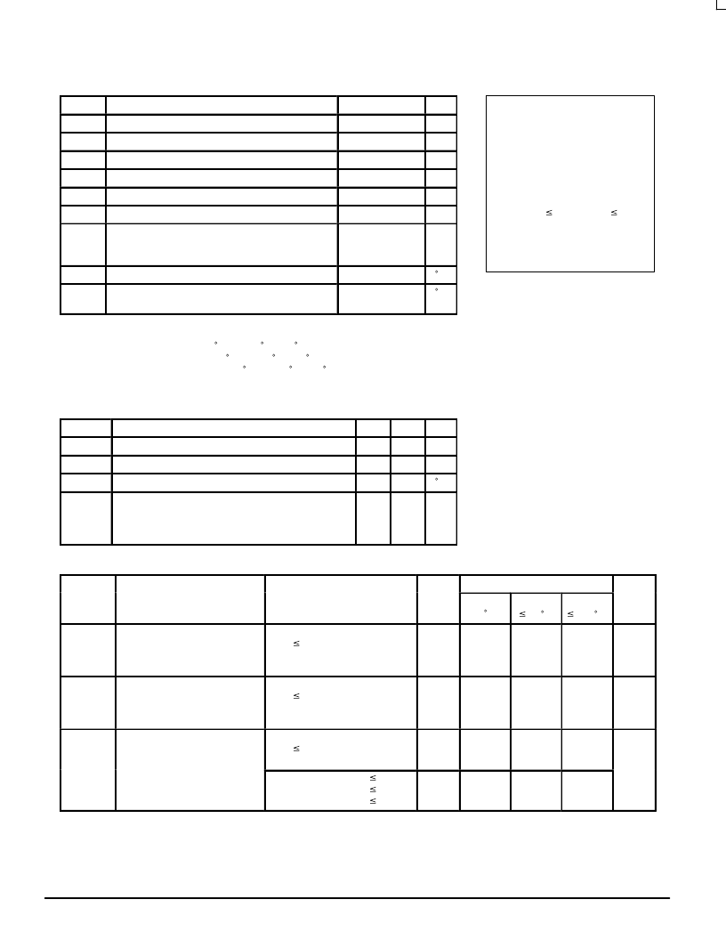
Functional operation should be restricted to the Recommended Operating Conditions.
Derating — Plastic DIP: – 10 mW/ C from 65 to 125 C
SOIC Package: –7 mW/ C from 65 to 125 C
TSSOP Package: – 6.1 mW/ C from 65 to 125 C
For high frequency or heavy load considerations, see Chapter 2 of the Motorola High–Speed CMOS Data Book (DL129/D).
Tstg
Storage Temperature
TL
Lead Temperature, 1 mm from Case for 10 Seconds
(Plastic DIP, SOIC or TSSOP Package)
V
450
mW
– 65 to + 150
C
C
RECOMMENDED OPERATING CONDITIONS
DC ELECTRICAL CHARACTERISTICS
(Voltages Referenced to GND)
DC Input Voltage, Output Voltage (Referenced to GND)
0
VCC
V
400
(Figure 1)
VCC = 3.0 V
0
0
1000
600
500
ns
VCC
25 C
85 C
Guaranteed Limit
5.2 mA
3.15
– 55 to
3.98
5.48
Minimum High–Level Input
Voltage
6.0
Vout = 0.1 V or VCC – 0.1 V
|Iout|
20
μ
A
4.5
0.9
1.8
3.15
3.15
Voltage
|Iout|
20
μ
A
3.0
0.9
0.9
Voltage
|Iout|
20
μ
A
4.5
1.9
4.4
3.70
5.20
4.4
4.4
V
Vin = VIH or VIL
|Iout|
|Iout|
|Iout|
4.5
6.0
3.84
5.34
This device contains protection
circuitry to guard against damage
due to high static voltages or electric
fields. However, precautions must
be taken to avoid applications of any
voltage higher than maximum rated
voltages to this high–impedance cir-
cuit. For proper operation, Vin and
Vout should be constrained to the
range GND
(Vin or Vout)
Unused inputs must always be
tied to an appropriate logic voltage
level (e.g., either GND or VCC).
Unused outputs must be left open.
VCC.
相关PDF资料 |
PDF描述 |
|---|---|
| MC74HC112D | Dual J-K Flip-Flop with Set and Reset |
| MC74HC11 | Dual J-K Flip-Flop with Set and Reset |
| MC74HC112DT | Dual J-K Flip-Flop with Set and Reset |
| MC74HC112N | Dual J-K Flip-Flop with Set and Reset |
| MC74HC11AD | Triple 3-Input AND Gate |
相关代理商/技术参数 |
参数描述 |
|---|---|
| MC74HC10ND | 制造商:Motorola Inc 功能描述: |
| MC74HC112ADG | 功能描述:触发器 DUAL J-K FLIP FLOP RoHS:否 制造商:Texas Instruments 电路数量:2 逻辑系列:SN74 逻辑类型:D-Type Flip-Flop 极性:Inverting, Non-Inverting 输入类型:CMOS 输出类型: 传播延迟时间:4.4 ns 高电平输出电流:- 16 mA 低电平输出电流:16 mA 电源电压-最大:5.5 V 最大工作温度:+ 85 C 安装风格:SMD/SMT 封装 / 箱体:X2SON-8 封装:Reel |
| MC74HC112ADR2G | 功能描述:触发器 DUAL J-K FLIP FLOP RoHS:否 制造商:Texas Instruments 电路数量:2 逻辑系列:SN74 逻辑类型:D-Type Flip-Flop 极性:Inverting, Non-Inverting 输入类型:CMOS 输出类型: 传播延迟时间:4.4 ns 高电平输出电流:- 16 mA 低电平输出电流:16 mA 电源电压-最大:5.5 V 最大工作温度:+ 85 C 安装风格:SMD/SMT 封装 / 箱体:X2SON-8 封装:Reel |
| MC74HC112ADTG | 功能描述:触发器 DUAL J-K FLIP FLOP RoHS:否 制造商:Texas Instruments 电路数量:2 逻辑系列:SN74 逻辑类型:D-Type Flip-Flop 极性:Inverting, Non-Inverting 输入类型:CMOS 输出类型: 传播延迟时间:4.4 ns 高电平输出电流:- 16 mA 低电平输出电流:16 mA 电源电压-最大:5.5 V 最大工作温度:+ 85 C 安装风格:SMD/SMT 封装 / 箱体:X2SON-8 封装:Reel |
| MC74HC112ADTR2G | 功能描述:触发器 DUAL J-K FLIP FLOP RoHS:否 制造商:Texas Instruments 电路数量:2 逻辑系列:SN74 逻辑类型:D-Type Flip-Flop 极性:Inverting, Non-Inverting 输入类型:CMOS 输出类型: 传播延迟时间:4.4 ns 高电平输出电流:- 16 mA 低电平输出电流:16 mA 电源电压-最大:5.5 V 最大工作温度:+ 85 C 安装风格:SMD/SMT 封装 / 箱体:X2SON-8 封装:Reel |
发布紧急采购,3分钟左右您将得到回复。