- 您现在的位置:买卖IC网 > PDF目录11431 > MC74HC4316ANG (ON Semiconductor)IC MUX/DEMUX QUAD 1X1 16DIP PDF资料下载
参数资料
| 型号: | MC74HC4316ANG |
| 厂商: | ON Semiconductor |
| 文件页数: | 7/11页 |
| 文件大小: | 0K |
| 描述: | IC MUX/DEMUX QUAD 1X1 16DIP |
| 标准包装: | 500 |
| 系列: | 74HC |
| 功能: | 多路复用器/多路分解器 |
| 电路: | 4 x 1:1 |
| 导通状态电阻: | 130 欧姆 |
| 电压电源: | 双电源 |
| 电压 - 电源,单路/双路(±): | ±2 V ~ 6 V |
| 电流 - 电源: | 40µA |
| 工作温度: | -55°C ~ 125°C |
| 安装类型: | 通孔 |
| 封装/外壳: | 16-DIP(0.300",7.62mm) |
| 供应商设备封装: | 16-DIP |
| 包装: | 管件 |
| 其它名称: | MC74HC4316ANG-ND MC74HC4316ANGOS |
MC74HC4316A
http://onsemi.com
5
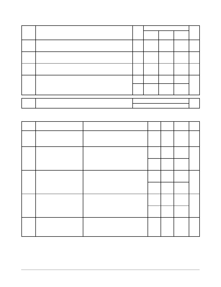
AC ELECTRICAL CHARACTERISTICS (CL = 50 pF, Control or Enable tr = tf = 6 ns, VEE = GND)
Symbol
Parameter
VCC
V
Guaranteed Limit
Unit
– 55 to
25°C
v 85°C
v 125°C
tPLH,
tPHL
Maximum Propagation Delay, Analog Input to Analog Output
2.0
4.5
6.0
40
6
5
50
8
7
60
9
8
ns
tPLZ,
tPHZ
Maximum Propagation Delay, Control or Enable to Analog Output
2.0
4.5
6.0
130
40
30
160
50
40
200
60
50
ns
tPZL,
tPZH
Maximum Propagation Delay, Control or Enable to Analog Output
2.0
4.5
6.0
140
40
30
175
50
40
250
60
50
ns
C
Maximum Capacitance
ON/OFF Control
and Enable Inputs
10
pF
Control Input = GND
Analog I/O
Feedthrough
35
1.0
35
1.0
35
1.0
CPD
Power Dissipation Capacitance (Per Switch) (Figure 14)*
Typical @ 25°C, VCC = 5.0 V
pF
15
*Used to determine the noload dynamic power consumption: PD = CPD VCC2f + ICC VCC.
ADDITIONAL APPLICATION CHARACTERISTICS (GND = 0 V)
Symbol
Parameter
Test Conditions
VCC
V
VEE
V
Limit*
25°C
Unit
BW
Maximum On–Channel Bandwidth
or
Minimum Frequency Response
(Figure 6)
fin = 1 MHz Sine Wave
Adjust fin Voltage to Obtain 0 dBm at VOS
Increase fin Frequency Until dB Meter
Reads – 3 dB
RL = 50 W, CL = 10 pF
2.25
4.50
6.00
– 2.25
– 4.50
– 6.00
150
160
MHz
Off–Channel Feedthrough
Isolation
(Figure 7)
fin Sine Wave
Adjust fin Voltage to Obtain 0 dBm at VIS
fin = 10 kHz, RL = 600 W, CL = 50 pF
2.25
4.50
6.00
– 2.25
– 4.50
– 6.00
– 50
dB
fin = 1.0 MHz, RL = 50 W, CL = 10 pF
2.25
4.50
6.00
– 2.25
– 4.50
– 6.00
– 40
Feedthrough Noise, Control to
Switch
(Figure 8)
Vin v 1 MHz Square Wave (tr = tf = 6 ns)
Adjust RL at Setup so that IS = 0 A
RL = 600 W, CL = 50 pF
2.25
4.50
6.00
– 2.25
– 4.50
– 6.00
30
65
100
mVPP
RL = 10 kW, CL = 10 pF
2.25
4.50
6.00
– 2.25
– 4.50
– 6.00
60
130
200
Crosstalk Between Any Two
Switches
(Figure 13)
fin Sine Wave
Adjust fin Voltage to Obtain 0 dBm at VIS
fin = 10 kHz, RL = 600 W, CL = 50 pF
2.25
4.50
6.00
– 2.25
– 4.50
– 6.00
– 70
dB
fin = 1.0 MHz, RL = 50 W, CL = 10 pF
2.25
4.50
6.00
– 2.25
– 4.50
– 6.00
– 80
THD
Total Harmonic Distortion
(Figure 15)
fin = 1 kHz, RL = 10 kW, CL = 50 pF
THD = THDMeasured THDSource
VIS = 4.0 VPP sine wave
VIS = 8.0 VPP sine wave
VIS = 11.0 VPP sine wave
2.25
4.50
6.00
– 2.25
– 4.50
– 6.00
0.10
0.06
0.04
%
*Limits not tested. Determined by design and verified by qualification.
相关PDF资料 |
PDF描述 |
|---|---|
| FSUSB42MUX | IC USB SWITCH DPDT 10MSOP |
| FSUSB46K8X | IC USB SWITCH DPST US8 |
| GRM2195C2AR40CD01D | CAP CER 0.4PF 100V NP0 0805 |
| GRM2195C2A9R9DZ01D | CAP CER 9.9PF 100V NP0 0805 |
| GRM2195C2A9R7DZ01D | CAP CER 9.7PF 100V NP0 0805 |
相关代理商/技术参数 |
参数描述 |
|---|---|
| MC74HC4316D | 制造商:Rochester Electronics LLC 功能描述:- Bulk |
| MC74HC4316DR2 | 制造商:ON Semiconductor 功能描述:Analog Switch Quad SPST 16-Pin SOIC T/R |
| MC74HC4316F | 制造商:Rochester Electronics LLC 功能描述:- Bulk |
| MC74HC4316FEL | 制造商:Rochester Electronics LLC 功能描述:- Bulk |
| MC74HC4316FL1 | 制造商:Rochester Electronics LLC 功能描述:- Bulk |
发布紧急采购,3分钟左右您将得到回复。