参数资料
| 型号: | MC74HC4538AFG |
| 厂商: | ON Semiconductor |
| 文件页数: | 10/16页 |
| 文件大小: | 0K |
| 描述: | IC MULTIVIBRATOR DUAL 16-SOEIAJ |
| 产品变化通告: | Product Discontinuation 30/Sept/2011 |
| 标准包装: | 50 |
| 系列: | 74HC |
| 逻辑类型: | 单稳态 |
| 独立电路: | 2 |
| 施密特触发器输入: | 是 |
| 传输延迟: | 30ns |
| 输出电流高,低: | 5.2mA,5.2mA |
| 电源电压: | 2 V ~ 6 V |
| 工作温度: | -55°C ~ 125°C |
| 安装类型: | 表面贴装 |
| 封装/外壳: | 16-SOIC(0.209",5.30mm 宽) |
| 供应商设备封装: | 16-SOEIAJ |
| 包装: | 管件 |
MC74HC4538A
http://onsemi.com
3
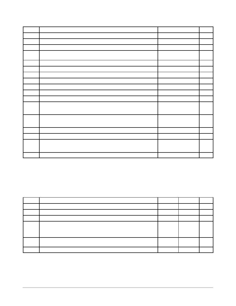
MAXIMUM RATINGS
Symbol
Parameter
Value
Unit
VCC
DC Supply Voltage
*0.5 to )7.0
V
VI
DC Input Voltage
*0.5 v VI v VCC )0.5
V
VO
DC Output Voltage
(Note 1)
*0.5 v VO v VCC )0.5
V
IIK
DC Input Diode Current
A, B, Reset
CX, RX
$20
$30
mA
IOK
DC Output Diode Current
$25
mA
IO
DC Output Sink Current
$25
mA
ICC
DC Supply Current per Supply Pin
$100
mA
IGND
DC Ground Current per Ground Pin
$100
mA
TSTG
Storage Temperature Range
*65 to )150
_C
TL
Lead temperature, 1 mm from Case for 10 Seconds
260
_C
TJ
Junction temperature under Bias
)150
_C
qJA
Thermal resistance
PDIP
SOIC
TSSOP
78
112
148
_C/W
PD
Power Dissipation in Still Air at 85
_C
PDIP
SOIC
TSSOP
750
500
450
mW
MSL
Moisture Sensitivity
Level 1
FR
Flammability Rating
Oxygen Index: 30% 35%
UL94VO (0.125 in)
VESD
ESD Withstand Voltage
Human Body Model (Note 2)
Machine Model (Note 3)
Charged Device Model (Note 4)
>2000
>100
>500
V
ILatchup
Latchup Performance
$300
mA
Stresses exceeding Maximum Ratings may damage the device. Maximum Ratings are stress ratings only. Functional operation above the
Recommended Operating Conditions is not implied. Extended exposure to stresses above the Recommended Operating Conditions may affect
device reliability.
1. IO absolute maximum rating must be observed.
2. Tested to EIA/JESD22A114A.
3. Tested to EIA/JESD22A115A.
4. Tested to JESD22C101A.
5. Tested to EIA/JESD78.
RECOMMENDED OPERATING CONDITIONS
Symbol
Parameter
Min
Max
Unit
VCC
DC Supply Voltage (Referenced to GND)
2.0
6.0
V
Vin, Vout
DC Input Voltage, Output Voltage (Referenced to GND)
0
VCC
V
TA
Operating Temperature, All Package Types
–55
+125
_C
tr, tf
Input Rise and Fall Time
VCC = 2.0 V
(Figure 7)
VCC = 4.5 V
VCC = 6.0 V
A or B (Figure 5)
0
1000
500
400
No Limit
ns
Rx
External Timing Resistor
VCC < 4.5 V
VCC ≥ 4.5 V
1.0
2.0
k
W
Cx
External Timing Capacitor
0
mF
The maximum allowable values of Rx and Cx are a function of the leakage of capacitor Cx, the leakage of the HC4538A, and leakage due to board layout
and surface resistance. For most applications, Cx/Rx should be limited to a maximum value of 10 mF/1.0 MW. Values of Cx >1.0 mF may cause a
problem during power down (see Power Down Considerations). Susceptibility to externally induced noise signals may occur for Rx >1.0 MW.
6. Unused inputs may not be left open. All inputs must be tied to a highlogic voltage level or a lowlogic input voltage level.
相关PDF资料 |
PDF描述 |
|---|---|
| MC74HC540AFG | IC INVERTER 8-INPUT 20SOEIAJ |
| MC74HC589AFELG | IC SHIFT REGISTER 8BIT 16-SOEIAJ |
| MC74HC595AFELG | IC SHIFT REGISTER 8BIT 16-SOEIAJ |
| MC74HC597ADTG | IC SHIFT REGISTER 8BIT 16TSSOP |
| MC74HC86AFG | IC GATE OR QUAD 2IN EXC 14SOEIAJ |
相关代理商/技术参数 |
参数描述 |
|---|---|
| MC74HC4538AFL1 | 制造商:Rochester Electronics LLC 功能描述:- Bulk |
| MC74HC4538AFL2 | 制造商:Rochester Electronics LLC 功能描述:- Bulk |
| MC74HC4538AFR1 | 制造商:Rochester Electronics LLC 功能描述:- Bulk |
| MC74HC4538AFR2 | 制造商:Rochester Electronics LLC 功能描述:- Bulk |
| MC74HC4538AN | 功能描述:单稳态多谐振荡器 3-6V Dual Precision RoHS:否 制造商:Texas Instruments 每芯片元件:1 逻辑系列:LVC 逻辑类型:Monostable Multivibrator 封装 / 箱体:SSOP-8 传播延迟时间:18.6 ns 高电平输出电流:- 32 mA 低电平输出电流:32 mA 电源电压-最大:5.5 V 电源电压-最小:1.65 V 最大功率耗散: 最大工作温度:+ 85 C 最小工作温度:- 40 C 封装:Reel |
发布紧急采购,3分钟左右您将得到回复。