参数资料
| 型号: | MC74HC597ADG |
| 厂商: | ON Semiconductor |
| 文件页数: | 8/12页 |
| 文件大小: | 0K |
| 描述: | IC SHIFT REGISTER 8BIT 16SOIC |
| 标准包装: | 48 |
| 系列: | 74HC |
| 逻辑类型: | 移位寄存器 |
| 输出类型: | 标准 |
| 元件数: | 1 |
| 每个元件的位元数: | 8 |
| 功能: | 串行至并行 |
| 电源电压: | 2 V ~ 6 V |
| 工作温度: | -55°C ~ 125°C |
| 安装类型: | 表面贴装 |
| 封装/外壳: | 16-SOIC(0.154",3.90mm 宽) |
| 供应商设备封装: | 16-SOIC |
| 包装: | 管件 |
MC74HC597A
http://onsemi.com
5
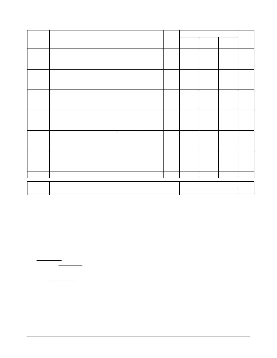
AC ELECTRICAL CHARACTERISTICS (CL = 50 pF, Input tr = tf = 6 ns)
Symbol
Parameter
VCC
V
Guaranteed Limit
Unit
– 55 to
25_C
v 85_C
v 125_C
fmax
Maximum Clock Frequency (50% Duty Cycle), Shift Clock
2.0
3.0
4.5
6.0
10
15
30
50
9
14
28
45
8
12
25
40
MHz
tPLH,
tPHL
Maximum Propagation Delay, Latch Clock to QH
2.0
3.0
4.5
6.0
175
100
40
30
225
110
50
40
275
125
60
50
ns
tPLH,
tPHL
Maximum Propagation Delay, Shift Clock to QH
2.0
3.0
4.5
6.0
160
90
30
25
200
130
40
30
240
160
48
40
ns
tPHL
Maximum Propagation Delay, Reset to QH
2.0
3.0
4.5
6.0
160
90
30
25
200
130
40
30
240
160
48
40
ns
tPLH,
tPHL
Maximum Propagation Delay, Serial Shift/Parallel Load to QH
2.0
3.0
4.5
6.0
160
90
30
25
200
130
40
30
240
160
48
40
ns
tTLH,
tTHL
Maximum Output Transition Time, Any Output
2.0
3.0
4.5
6.0
75
27
15
13
95
32
19
16
110
36
22
19
ns
Cin
Maximum Input Capacitance
—
10
pF
CPD
Power Dissipation Capacitance (Per Package)*
Typical @ 25°C, VCC = 5.0 V
pF
40
* Used to determine the noload dynamic power consumption: PD = CPD VCC2f + ICC VCC.
PIN DESCRIPTIONS
DATA INPUTS
A, B, C, D, E, F, G, H (Pins 15, 1, 2, 3, 4, 5, 6, 7)
Parallel data inputs. Data on these inputs is stored in the
input latch on the rising edge of the Latch Clock input.
SA (Pin 14)
Serial data input. Data on this input is shifted into the shift
register on the rising edge of the Shift Clock input it Serial
Shift/Parallel Load is high. Data on this input is ignored
when Serial Shift/Parallel Load is low.
CONTROL INPUTS
Serial Shift/Parallel Load (Pin 13)
Shift register mode control. When a high level is applied
to this pin, the shift register is allowed to serially shift data.
When a low level is applied to this pin, the shift register
accepts parallel data from the input latch, and serial shifting
is inhibited.
Reset (Pin 10)
Asynchronous, Activelow shift register reset. A low level
applied to this input resets the shift register to a low level,
but does not change the data in the input latch.
Shift Clock (Pin 11)
Serial shift register clock. A lowtohigh transition on this
input shifts data on the Serial Data Input into the shift
register and data in stage H is shifted out QH, being
replaced by the data previously stored in stage G.
Latch Clock (Pin 12)
Latch clock. A lowtohigh transition on this input loads
the parallel data on inputs AH into the input latch.
OUTPUT
QH (Pin 9)
Serial data output. This pin is the output from the last
stage of the shift register.
相关PDF资料 |
PDF描述 |
|---|---|
| MC74VHC04DR2G | IC INVERTER HEX ADV HS 14-SOIC |
| MC74HCT4094ADR2G | IC BUS REG TRE-ST 8STG 16SOIC |
| MC74VHC02DTR2G | IC GATE NOR QUAD 2INPUT 14-TSSOP |
| 153X | THICK PANEL/GOLD PLA |
| MC74VHC00DR2G | IC GATE NAND QUAD 2INP 14-SOIC |
相关代理商/技术参数 |
参数描述 |
|---|---|
| MC74HC597ADR2 | 制造商:Rochester Electronics LLC 功能描述:- Bulk 制造商:Motorola Inc 功能描述: 制造商:MOTOROLA 功能描述: |
| MC74HC597ADR2G | 功能描述:计数器移位寄存器 IC SHIFT REGISTER 8-BIT RoHS:否 制造商:Texas Instruments 计数器类型: 计数顺序:Serial to Serial/Parallel 电路数量:1 封装 / 箱体:SOIC-20 Wide 逻辑系列: 逻辑类型: 输入线路数量:1 输出类型:Open Drain 传播延迟时间:650 ns 最大工作温度:+ 125 C 最小工作温度:- 40 C 封装:Reel |
| MC74HC597ADTG | 功能描述:计数器移位寄存器 RoHS:否 制造商:Texas Instruments 计数器类型: 计数顺序:Serial to Serial/Parallel 电路数量:1 封装 / 箱体:SOIC-20 Wide 逻辑系列: 逻辑类型: 输入线路数量:1 输出类型:Open Drain 传播延迟时间:650 ns 最大工作温度:+ 125 C 最小工作温度:- 40 C 封装:Reel |
| MC74HC597ADTR2G | 功能描述:计数器移位寄存器 IC SHIFT REGISTER 8-BIT RoHS:否 制造商:Texas Instruments 计数器类型: 计数顺序:Serial to Serial/Parallel 电路数量:1 封装 / 箱体:SOIC-20 Wide 逻辑系列: 逻辑类型: 输入线路数量:1 输出类型:Open Drain 传播延迟时间:650 ns 最大工作温度:+ 125 C 最小工作温度:- 40 C 封装:Reel |
| MC74HC597AF | 制造商:Rochester Electronics LLC 功能描述:- Bulk |
发布紧急采购,3分钟左右您将得到回复。