- 您现在的位置:买卖IC网 > PDF目录26807 > MC74HC597AN (ON SEMICONDUCTOR) HC/UH SERIES, 8-BIT RIGHT PARALLEL IN SERIAL OUT SHIFT REGISTER, TRUE OUTPUT, PDIP16 PDF资料下载
参数资料
| 型号: | MC74HC597AN |
| 厂商: | ON SEMICONDUCTOR |
| 元件分类: | 计数移位寄存器 |
| 英文描述: | HC/UH SERIES, 8-BIT RIGHT PARALLEL IN SERIAL OUT SHIFT REGISTER, TRUE OUTPUT, PDIP16 |
| 封装: | PLASTIC, DIP-16 |
| 文件页数: | 5/11页 |
| 文件大小: | 291K |
| 代理商: | MC74HC597AN |
MC54/74HC597A
High–Speed CMOS Logic Data
DL129 — Rev 6
3
MOTOROLA
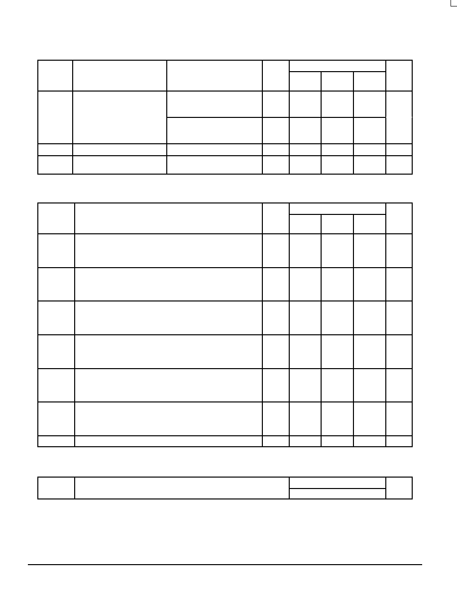
DC ELECTRICAL CHARACTERISTICS (Voltages Referenced to GND)
Unit
Guaranteed Limit
VCC
V
Test Conditions
Parameter
Symbol
Unit
v 125_C
v 85_C
– 55 to
25
_C
VCC
V
Test Conditions
Parameter
Symbol
VOL
Maximum Low–Level Output
Voltage
Vin = VIH or VIL
|Iout| v 20 A
2.0
4.5
6.0
0.1
0.1
0.1
V
Vin = VIH or VIL |Iout| v 2.4 mA
|Iout| v 4.0 mA
|Iout| v 5.2 mA
3.0
4.5
6.0
0.26
0.33
0.40
Iin
Maximum Input Leakage Current
Vin = VCC or GND
6.0
± 0.1
± 1.0
± 1.0
A
ICC
Maximum Quiescent Supply
Current (per Package)
Vin = VCC or GND
Iout = 0 A
6.0
4
40
160
A
NOTE: Information on typical parametric values can be found in Chapter 2 of the Motorola High–Speed CMOS Data Book (DL129/D).
AC ELECTRICAL CHARACTERISTICS (CL = 50 pF, Input tr = tf = 6 ns)
Symbol
Parameter
VCC
V
Guaranteed Limit
Unit
Symbol
Parameter
VCC
V
– 55 to
25
_C
v 85_C
v 125_C
Unit
fmax
Maximum Clock Frequency (50% Duty Cycle)
(Figures 2 and 8)
2.0
3.0
4.5
6.0
10
15
30
50
9
14
28
45
8
12
25
40
MHz
tPLH,
tPHL
Maximum Propagation Delay, Latch Clock to QH
(Figures 1 and 8)
2.0
3.0
4.5
6.0
175
100
40
30
225
110
50
40
275
125
60
50
ns
tPLH,
tPHL
Maximum Propagation Delay, Shift Clock to QH
(Figures 2 and 8)
2.0
3.0
4.5
6.0
160
90
30
25
200
130
40
30
240
160
48
40
ns
tPHL
Maximum Propagation Delay, Reset to QH
(Figures 3 and 8)
2.0
3.0
4.5
6.0
160
90
30
25
200
130
40
30
240
160
48
40
ns
tPLH,
tPHL
Maximum Propagation Delay, Serial Shift/Parallel Load to QH
(Figures 4 and 8)
2.0
3.0
4.5
6.0
160
90
30
25
200
130
40
30
240
160
48
40
ns
tTLH,
tTHL
Maximum Output Transition Time, Any Output
(Figures 1 and 8)
2.0
3.0
4.5
6.0
75
27
15
13
95
32
19
16
110
36
22
19
ns
Cin
Maximum Input Capacitance
—
10
10
10
pF
NOTES:
1. For propagation delays with loads other than 50 pF, see Chapter 2 of the Motorola High–Speed CMOS Data Book (DL129/D).
2. Information on typical parametric values can be found in Chapter 2 of the Motorola High–Speed CMOS Data Book (DL129/D).
CPD
Power Dissipation Capacitance (Per Package)*
Typical @ 25
°C, VCC = 5.0 V
pF
CPD
Power Dissipation Capacitance (Per Package)*
40
pF
* Used to determine the no–load dynamic power consumption: PD = CPD VCC2f + ICC VCC. For load considerations, see Chapter 2 of the
Motorola High–Speed CMOS Data Book (DL129/D).
相关PDF资料 |
PDF描述 |
|---|---|
| MC74HC597ADTR2 | HC/UH SERIES, 8-BIT RIGHT PARALLEL IN SERIAL OUT SHIFT REGISTER, TRUE OUTPUT, PDSO16 |
| MC74HC646DWR2 | HC/UH SERIES, 8-BIT REGISTERED TRANSCEIVER, TRUE OUTPUT, PDSO24 |
| MC74HC7266DDR2 | HC/UH SERIES, QUAD 2-INPUT XNOR GATE, PDSO14 |
| MC54HC7266JD | HC/UH SERIES, QUAD 2-INPUT XNOR GATE, CDIP14 |
| MC74HC74AND | HC/UH SERIES, DUAL POSITIVE EDGE TRIGGERED D FLIP-FLOP, COMPLEMENTARY OUTPUT, PDIP14 |
相关代理商/技术参数 |
参数描述 |
|---|---|
| MC74HC597D | 制造商:Motorola Inc 功能描述: |
| MC74HC597N | 制造商:Motorola Inc 功能描述: 制造商:Motorola Inc 功能描述:Shift Register, 16 Pin, Plastic, DIP |
| MC74HC640ADT | 制造商:Rochester Electronics LLC 功能描述:- Tape and Reel 制造商:ON Semiconductor 功能描述: |
| MC74HC640ADTEL | 制造商:Rochester Electronics LLC 功能描述:- Bulk 制造商:Motorola Inc 功能描述: 制造商:MOTOROLA 功能描述: |
| MC74HC640ADW | 制造商:Motorola Inc 功能描述:Bus Transceiver, Single, 8 Bit, 20 Pin, Plastic, SOP |
发布紧急采购,3分钟左右您将得到回复。