参数资料
| 型号: | MC74HC73ADR2G |
| 厂商: | ON Semiconductor |
| 文件页数: | 2/7页 |
| 文件大小: | 0K |
| 描述: | IC DUAL J-K FLPFLP W/REST 14SOIC |
| 标准包装: | 2,500 |
| 系列: | 74HC |
| 功能: | 复位 |
| 类型: | JK 型 |
| 输出类型: | 差分 |
| 元件数: | 2 |
| 每个元件的位元数: | 2 |
| 频率 - 时钟: | 35MHz |
| 延迟时间 - 传输: | 21ns |
| 触发器类型: | 负边沿 |
| 输出电流高,低: | 5.2mA,5.2mA |
| 电源电压: | 2 V ~ 6 V |
| 工作温度: | -55°C ~ 125°C |
| 安装类型: | 表面贴装 |
| 封装/外壳: | 14-SOIC(0.154",3.90mm 宽) |
| 包装: | 带卷 (TR) |
MC74HC73A
http://onsemi.com
2
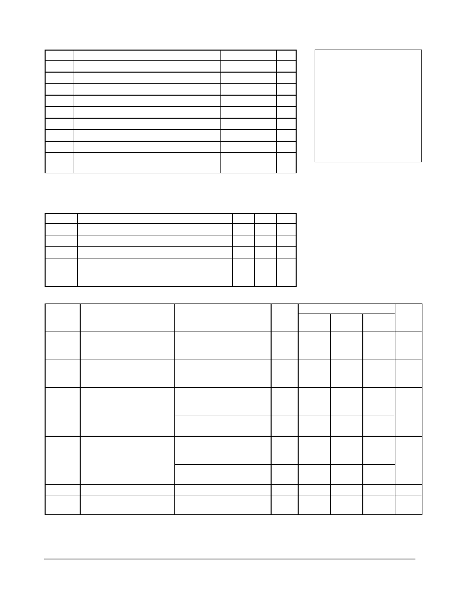
MAXIMUM RATINGS*
Symbol
Parameter
Value
Unit
VCC
DC Supply Voltage (Referenced to GND)
– 0.5 to + 7.0
V
Vin
DC Input Voltage (Referenced to GND)
– 1.5 to VCC + 1.5
V
Vout
DC Output Voltage (Referenced to GND)
– 0.5 to VCC + 0.5
V
Iin
DC Input Current, per Pin
± 20
mA
Iout
DC Output Current, per Pin
± 25
mA
ICC
DC Supply Current, VCC and GND Pins
± 50
mA
PD
Power Dissipation in Still Air
SOIC Package
500
mW
Tstg
Storage Temperature
– 65 to + 150
_C
TL
Lead Temperature, 1 mm from Case for 10 Seconds
(PSOIC Package)
260
_C
*Maximum Ratings are those values beyond which damage to the device may occur.
Functional operation should be restricted to the Recommended Operating Conditions.
Derating — SOIC Package: – 7 mW/_C from 65_ to 125_C
RECOMMENDED OPERATING CONDITIONS
Symbol
Parameter
Min
Max
Unit
VCC
DC Supply Voltage (Referenced to GND)
2.0
6.0
V
Vin, Vout
DC Input Voltage, Output Voltage (Referenced to GND)
0
VCC
V
TA
Operating Temperature, All Package Types
– 55
+ 125
_C
tr, tf
Input Rise and Fall Time
VCC = 2.0 V
(Figure 1)
VCC = 4.5 V
VCC = 6.0 V
0
1000
500
400
ns
DC ELECTRICAL CHARACTERISTICS (Voltages Referenced to GND)
Symbol
Parameter
Test Conditions
VCC
V
Guaranteed Limit
Unit
– 55 to
25_C
v 85_C
v 125_C
VIH
Minimum HighLevel Input
Voltage
Vout = 0.1 V or VCC – 0.1 V
|Iout| v 20 μA
2.0
4.5
6.0
1.5
3.15
4.2
1.5
3.15
4.2
1.5
3.15
4.2
V
VIL
Maximum LowLevel Input
Voltage
Vout = 0.1 V or VCC – 0.1 V
|Iout| v 20 μA
2.0
4.5
6.0
0.3
0.9
1.2
0.3
0.9
1.2
0.3
0.9
1.2
V
VOH
Minimum HighLevel Output
Voltage
Vin = VIH or VIL
|Iout| v 20 μA
2.0
4.5
6.0
1.9
4.4
5.9
1.9
4.4
5.9
1.9
4.4
5.9
V
Vin = VIH or VIL
|Iout| v 4.0 mA
|Iout| v 5.2 mA
4.5
6.0
3.98
5.48
3.84
5.34
3.70
5.20
VOL
Maximum LowLevel Output
Voltage
Vin = VIH or VIL
|Iout| v 20 μA
2.0
4.5
6.0
0.1
V
Vin = VIH or VIL
|Iout| v 4.0 mA
|Iout| v 5.2 mA
4.5
6.0
0.26
0.33
0.40
Iin
Maximum Input Leakage Current Vin = VCC or GND
6.0
± 0.1
± 1.0
μA
ICC
Maximum Quiescent Supply
Current (per Package)
Vin = VCC or GND
Iout = 0 μA
6.0
4
40
80
μA
This device contains protection
circuitry to guard against damage
due to high static voltages or electric
fields. However, precautions must
be taken to avoid applications of any
voltage higher than maximum rated
voltages to this highimpedance cir-
cuit. For proper operation, Vin and
Vout should be constrained to the
range GND v (Vin or Vout) v VCC.
Unused inputs must always be
tied to an appropriate logic voltage
level (e.g., either GND or VCC).
Unused outputs must be left open.
相关PDF资料 |
PDF描述 |
|---|---|
| VE-2NH-MV-F2 | CONVERTER MOD DC/DC 52V 150W |
| MC74HC73ADG | IC DUAL J-K FLPFLP W/REST 14SOIC |
| VE-2NF-MV-F3 | CONVERTER MOD DC/DC 72V 150W |
| RSZ-1512/H-R | CONV DC/DC 1W 15VIN 12VOUT |
| RSZ-1512/H | CONV DC/DC 1W 15VIN 12VOUT |
相关代理商/技术参数 |
参数描述 |
|---|---|
| MC74HC73ADTG | 功能描述:触发器 DUAL J-K FLIPFLOP W RESET RoHS:否 制造商:Texas Instruments 电路数量:2 逻辑系列:SN74 逻辑类型:D-Type Flip-Flop 极性:Inverting, Non-Inverting 输入类型:CMOS 输出类型: 传播延迟时间:4.4 ns 高电平输出电流:- 16 mA 低电平输出电流:16 mA 电源电压-最大:5.5 V 最大工作温度:+ 85 C 安装风格:SMD/SMT 封装 / 箱体:X2SON-8 封装:Reel |
| MC74HC73ADTR2G | 功能描述:触发器 DUAL J-K FLIPFLOP W RESET RoHS:否 制造商:Texas Instruments 电路数量:2 逻辑系列:SN74 逻辑类型:D-Type Flip-Flop 极性:Inverting, Non-Inverting 输入类型:CMOS 输出类型: 传播延迟时间:4.4 ns 高电平输出电流:- 16 mA 低电平输出电流:16 mA 电源电压-最大:5.5 V 最大工作温度:+ 85 C 安装风格:SMD/SMT 封装 / 箱体:X2SON-8 封装:Reel |
| MC74HC73F | 制造商:ON Semiconductor 功能描述: |
| MC74HC73N | 制造商:Motorola Inc 功能描述: |
| MC74HC74AD | 功能描述:触发器 2-6V CMOS Dual RoHS:否 制造商:Texas Instruments 电路数量:2 逻辑系列:SN74 逻辑类型:D-Type Flip-Flop 极性:Inverting, Non-Inverting 输入类型:CMOS 输出类型: 传播延迟时间:4.4 ns 高电平输出电流:- 16 mA 低电平输出电流:16 mA 电源电压-最大:5.5 V 最大工作温度:+ 85 C 安装风格:SMD/SMT 封装 / 箱体:X2SON-8 封装:Reel |
发布紧急采购,3分钟左右您将得到回复。