- 您现在的位置:买卖IC网 > PDF目录26807 > MC74HCT125ADG (ON SEMICONDUCTOR) OTHER DECODER/DRIVER, PDSO14 PDF资料下载
参数资料
| 型号: | MC74HCT125ADG |
| 厂商: | ON SEMICONDUCTOR |
| 元件分类: | 编、解码器及复用、解复用 |
| 英文描述: | OTHER DECODER/DRIVER, PDSO14 |
| 封装: | LEAD FREE, SOIC-14 |
| 文件页数: | 2/8页 |
| 文件大小: | 163K |
| 代理商: | MC74HCT125ADG |
MC74HCT125A
http://onsemi.com
2
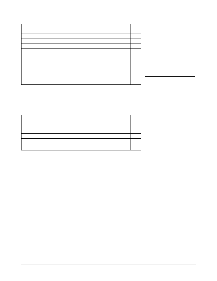
MAXIMUM RATINGS
Symbol
Parameter
Value
Unit
VCC
DC Supply Voltage (Referenced to GND)
– 0.5 to + 7.0
V
Vin
DC Input Voltage (Referenced to GND)
– 0.5 to VCC + 0.5
V
Vout
DC Output Voltage (Referenced to GND)
– 0.5 to VCC + 0.5
V
Iin
DC Input Current, per Pin
± 20
mA
Iout
DC Output Current, per Pin
± 35
mA
ICC
DC Supply Current, VCC and GND Pins
± 75
mA
PD
Power Dissipation in Still Air
Plastic DIP
SOIC Package
TSSOP Package
750
500
450
mW
Tstg
Storage Temperature
– 65 to + 150
_C
TL
Lead Temperature, 1 mm from Case for 10 Seconds
(Plastic DIP, SOIC or TSSOP Package)
260
_C
Stresses exceeding Maximum Ratings may damage the device. Maximum Ratings are stress
ratings only. Functional operation above the Recommended Operating Conditions is not implied.
Extended exposure to stresses above the Recommended Operating Conditions may affect device
reliability.
Derating — Plastic DIP: – 10 mW/_C from 65_ to 125_C
SOIC Package: – 7 mW/_C from 65_ to 125_C
TSSOP Package: – 6.1 mW/_C from 65_ to 125_C
RECOMMENDED OPERATING CONDITIONS
Symbol
Parameter
Min
Max
Unit
VCC
DC Supply Voltage (Referenced to GND)
2.0
6.0
V
Vin, Vout DC Input Voltage, Output Voltage
(Referenced to GND)
0
VCC
V
TA
Operating Temperature, All Package Types
– 55
+ 125
_C
tr, tf
Input Rise and Fall Time
VCC = 2.0 V
(Figure 1)
VCC = 4.5 V
VCC = 6.0 V
0
1000
500
400
ns
This device contains protection
circuitry to guard against damage
due to high static voltages or electric
fields. However, precautions must
be taken to avoid applications of any
voltage higher than maximum rated
voltages to this highimpedance cir-
cuit. For proper operation, Vin and
Vout should be constrained to the
range GND v (Vin or Vout) v VCC.
Unused inputs must always be
tied to an appropriate logic voltage
level (e.g., either GND or VCC).
Unused outputs must be left open.
相关PDF资料 |
PDF描述 |
|---|---|
| MC74HCT125AFELG | OTHER DECODER/DRIVER, PDSO14 |
| MC74HCT125ADTR2G | OTHER DECODER/DRIVER, PDSO14 |
| MC74HCT132AFELG | NAND GATE, PDSO14 |
| MC74HCT132ANG | NAND GATE, PDIP14 |
| MC74HCT174AD | HCT SERIES, POSITIVE EDGE TRIGGERED D FLIP-FLOP, TRUE OUTPUT, PDSO16 |
相关代理商/技术参数 |
参数描述 |
|---|---|
| MC74HCT125ADR2G | 功能描述:缓冲器和线路驱动器 BUFF/DVR TRI-ST QD RoHS:否 制造商:Micrel 输入线路数量:1 输出线路数量:2 极性:Non-Inverting 电源电压-最大:+/- 5.5 V 电源电压-最小:+/- 2.37 V 最大工作温度:+ 85 C 安装风格:SMD/SMT 封装 / 箱体:MSOP-8 封装:Reel |
| MC74HCT125ADTG | 功能描述:缓冲器和线路驱动器 BUFF/DVR TRI-ST QD RoHS:否 制造商:Micrel 输入线路数量:1 输出线路数量:2 极性:Non-Inverting 电源电压-最大:+/- 5.5 V 电源电压-最小:+/- 2.37 V 最大工作温度:+ 85 C 安装风格:SMD/SMT 封装 / 箱体:MSOP-8 封装:Reel |
| MC74HCT125ADTR2G | 功能描述:缓冲器和线路驱动器 BUFF/DVR TRI-ST QD RoHS:否 制造商:Micrel 输入线路数量:1 输出线路数量:2 极性:Non-Inverting 电源电压-最大:+/- 5.5 V 电源电压-最小:+/- 2.37 V 最大工作温度:+ 85 C 安装风格:SMD/SMT 封装 / 箱体:MSOP-8 封装:Reel |
| MC74HCT132ADG | 功能描述:逻辑门 IC QUAD 2-IN NAND GATE HS RoHS:否 制造商:Texas Instruments 产品:OR 逻辑系列:LVC 栅极数量:2 线路数量(输入/输出):2 / 1 高电平输出电流:- 16 mA 低电平输出电流:16 mA 传播延迟时间:3.8 ns 电源电压-最大:5.5 V 电源电压-最小:1.65 V 最大工作温度:+ 125 C 安装风格:SMD/SMT 封装 / 箱体:DCU-8 封装:Reel |
| MC74HCT132ADR2G | 功能描述:逻辑门 IC QUAD 2-IN NAND GATE HS RoHS:否 制造商:Texas Instruments 产品:OR 逻辑系列:LVC 栅极数量:2 线路数量(输入/输出):2 / 1 高电平输出电流:- 16 mA 低电平输出电流:16 mA 传播延迟时间:3.8 ns 电源电压-最大:5.5 V 电源电压-最小:1.65 V 最大工作温度:+ 125 C 安装风格:SMD/SMT 封装 / 箱体:DCU-8 封装:Reel |
发布紧急采购,3分钟左右您将得到回复。