- 您现在的位置:买卖IC网 > PDF目录11199 > MC74HCT4051ADR2G (ON Semiconductor)ANALOG MULTIPLEXERS/DEMU SOIC16 PDF资料下载
参数资料
| 型号: | MC74HCT4051ADR2G |
| 厂商: | ON Semiconductor |
| 文件页数: | 2/16页 |
| 文件大小: | 0K |
| 描述: | ANALOG MULTIPLEXERS/DEMU SOIC16 |
| 标准包装: | 2,500 |
| 系列: | 74HCT |
| 功能: | 多路复用器/多路分解器 |
| 电路: | 1 x 8:1 |
| 导通状态电阻: | 100 欧姆 |
| 电压电源: | 单电源 |
| 电压 - 电源,单路/双路(±): | 2 V ~ 6 V |
| 电流 - 电源: | 1µA |
| 工作温度: | -55°C ~ 125°C |
| 安装类型: | 表面贴装 |
| 封装/外壳: | 16-SOIC(0.295",7.50mm 宽) |
| 供应商设备封装: | 16-SOIC W |
| 包装: | 带卷 (TR) |
MC74HCT4051A, MC74HCT4052A, MC74HCT4053A
http://onsemi.com
10
RL
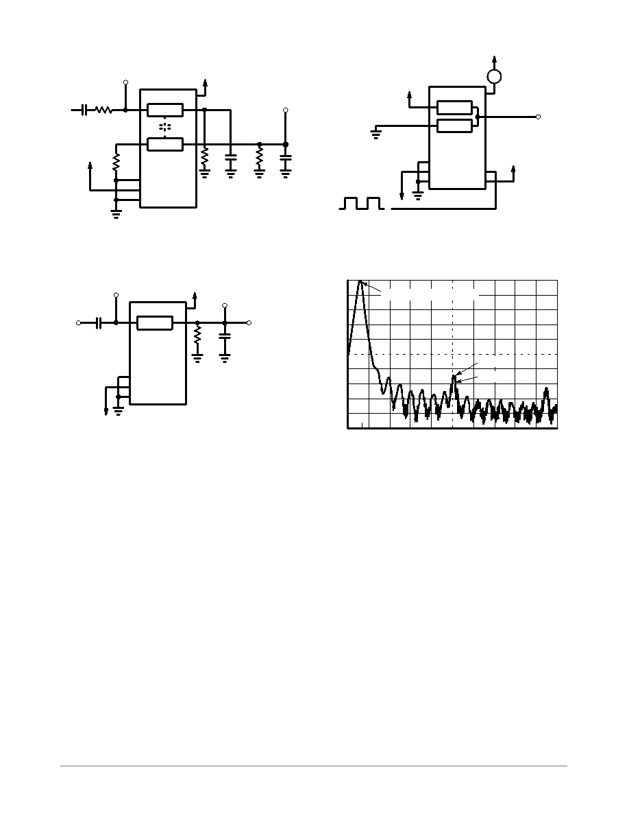
Figure 18. Crosstalk Between Any Two
Switches, Test SetUp
Figure 19. Power Dissipation Capacitance,
Test SetUp
Figure 20a. Total Harmonic Distortion, Test SetUp
Figure 20b. Plot, Harmonic Distortion
0
-10
-20
-30
-40
-50
- 100
1.0
2.0
3.125
FREQUENCY (kHz)
dB
-60
-70
-80
-90
FUNDAMENTAL FREQUENCY
DEVICE
SOURCE
ON
6
7
8
16
VEE
CL*
*Includes all probe and jig capacitance
OFF
RL
VIS
RL
CL*
VOS
fin
0.1
mF
ON/OFF
6
7
8
16
VCC
CHANNEL SELECT
NC
COMMON O/I
OFF/ON
ANALOG I/O
VCC
A
11
VCC
VEE
ON
6
7
8
16
VCC
VEE
0.1
mF
CL*
fin
RL
TO
DISTORTION
METER
*Includes all probe and jig capacitance
VOS
VIS
Figure 20.
APPLICATIONS INFORMATION
The maximum analog voltage swings are determined by
the supply voltages VCC and VEE. The positive peak analog
voltage should not exceed VCC. Similarly, the negative peak
analog voltage should not go below VEE. In this example,
the difference between VCC and VEE is ten volts. Therefore,
using the configuration of Figure 21, a maximum analog
signal of ten volts peaktopeak can be controlled. Unused
analog inputs/outputs may be left floating (i.e., not
connected). However, tying unused analog inputs and
outputs to VCC or GND through a low value resistor helps
minimize crosstalk and feedthrough noise that may be
picked up by an unused switch.
Although used here, balanced supplies are not a
requirement. The only constraints on the power supplies are
that:
VCC GND = 2 to 6 V
VEE GND = 0 to 6 V
VCC VEE = 2 to 12 V
and VEE ≤ GND
When voltage transients above VCC and/or below VEE are
anticipated on the analog channels, external Germanium or
Schottky diodes (Dx) are recommended as shown in
Figure 22. These diodes should be able to absorb the
maximum anticipated current surges during clipping.
相关PDF资料 |
PDF描述 |
|---|---|
| VE-B4P-IX | CONVERTER MOD DC/DC 13.8V 75W |
| ATMEGA128-16AUR | MCU AVR 128KB FLASH 16MHZ 64TQFP |
| M74HCT4051ADTR2G | ANALOG MULTIPLEXERS/DEMU TSSOP16 |
| ADUC848BSZ32-5 | IC MCU FLASH W/16BIT ADC 52MQFP |
| ADUC842BCPZ8-5 | IC MCU 8KB FLASH ADC/DAC 56LFCSP |
相关代理商/技术参数 |
参数描述 |
|---|---|
| MC74HCT4051ADTG | 功能描述:编码器、解码器、复用器和解复用器 ANALOG MULTI PLEXERS/DEMU RoHS:否 制造商:Micrel 产品:Multiplexers 逻辑系列:CMOS 位数: 线路数量(输入/输出):2 / 12 传播延迟时间:350 ps, 400 ps 电源电压-最大:2.625 V, 3.6 V 电源电压-最小:2.375 V, 3 V 最大工作温度:+ 85 C 安装风格:SMD/SMT 封装 / 箱体:QFN-44 封装:Tray |
| MC74HCT4066ADG | 功能描述:编码器、解码器、复用器和解复用器 RoHS:否 制造商:Micrel 产品:Multiplexers 逻辑系列:CMOS 位数: 线路数量(输入/输出):2 / 12 传播延迟时间:350 ps, 400 ps 电源电压-最大:2.625 V, 3.6 V 电源电压-最小:2.375 V, 3 V 最大工作温度:+ 85 C 安装风格:SMD/SMT 封装 / 箱体:QFN-44 封装:Tray |
| MC74HCT4066ADR2G | 功能描述:编码器、解码器、复用器和解复用器 RoHS:否 制造商:Micrel 产品:Multiplexers 逻辑系列:CMOS 位数: 线路数量(输入/输出):2 / 12 传播延迟时间:350 ps, 400 ps 电源电压-最大:2.625 V, 3.6 V 电源电压-最小:2.375 V, 3 V 最大工作温度:+ 85 C 安装风格:SMD/SMT 封装 / 箱体:QFN-44 封装:Tray |
| MC74HCT4066ADTG | 功能描述:编码器、解码器、复用器和解复用器 RoHS:否 制造商:Micrel 产品:Multiplexers 逻辑系列:CMOS 位数: 线路数量(输入/输出):2 / 12 传播延迟时间:350 ps, 400 ps 电源电压-最大:2.625 V, 3.6 V 电源电压-最小:2.375 V, 3 V 最大工作温度:+ 85 C 安装风格:SMD/SMT 封装 / 箱体:QFN-44 封装:Tray |
| MC74HCT4094ADG | 功能描述:计数器移位寄存器 IC BUS REG TRE-ST 8STG RoHS:否 制造商:Texas Instruments 计数器类型: 计数顺序:Serial to Serial/Parallel 电路数量:1 封装 / 箱体:SOIC-20 Wide 逻辑系列: 逻辑类型: 输入线路数量:1 输出类型:Open Drain 传播延迟时间:650 ns 最大工作温度:+ 125 C 最小工作温度:- 40 C 封装:Reel |
发布紧急采购,3分钟左右您将得到回复。