- 您现在的位置:买卖IC网 > PDF目录11193 > MC74HCT4851ADTG (ON Semiconductor)ANALOG MULTIPLEXERS/DEMUL TSSOP PDF资料下载
参数资料
| 型号: | MC74HCT4851ADTG |
| 厂商: | ON Semiconductor |
| 文件页数: | 8/14页 |
| 文件大小: | 0K |
| 描述: | ANALOG MULTIPLEXERS/DEMUL TSSOP |
| 标准包装: | 96 |
| 系列: | 74HCT |
| 功能: | 多路复用器/多路分解器 |
| 电路: | 1 x 8:1 |
| 导通状态电阻: | 400 欧姆 |
| 电压电源: | 单电源 |
| 电压 - 电源,单路/双路(±): | 2 V ~ 6 V |
| 电流 - 电源: | 2µA |
| 工作温度: | -55°C ~ 125°C |
| 安装类型: | 表面贴装 |
| 封装/外壳: | 16-TSSOP(0.173",4.40mm 宽) |
| 供应商设备封装: | 16-TSSOP |
| 包装: | 管件 |
MC74HCT4851A, MC74HCT4852A
http://onsemi.com
3
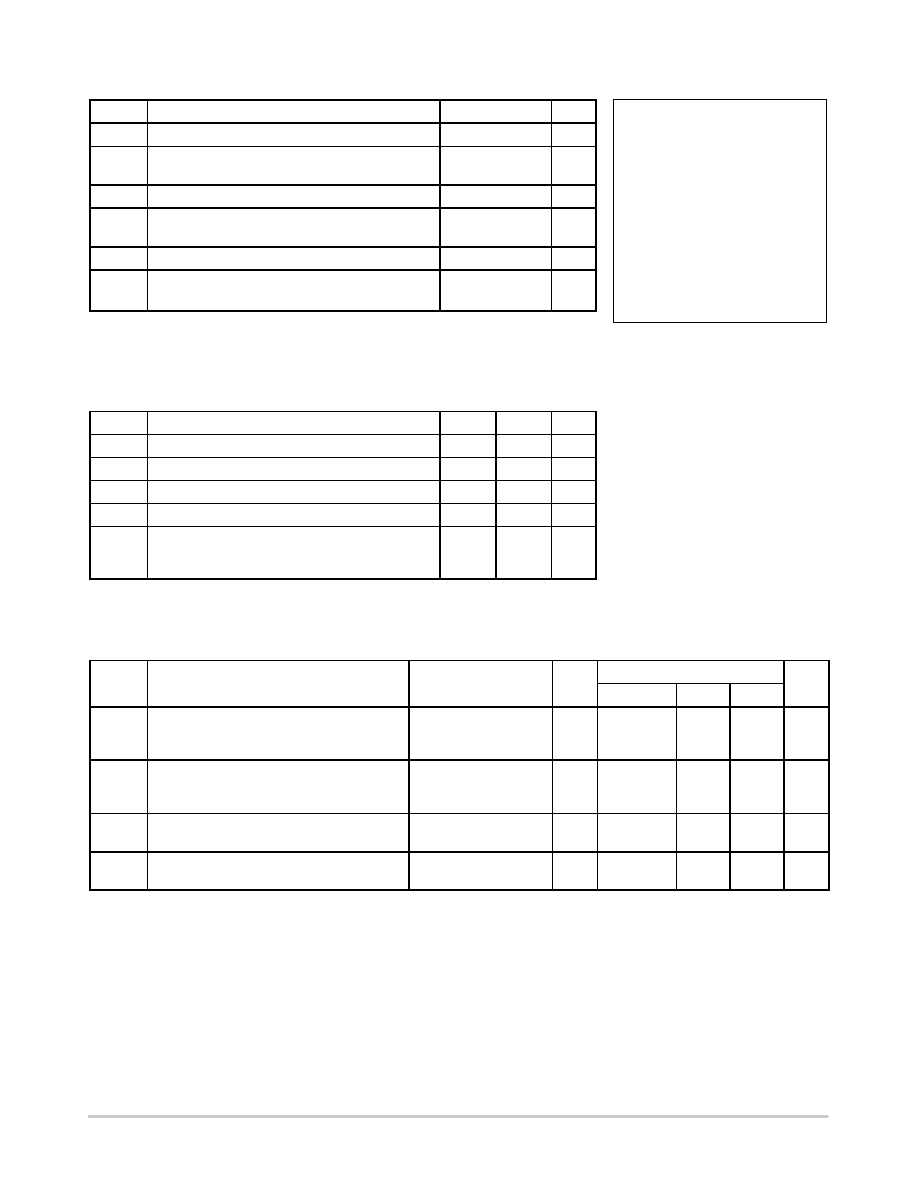
MAXIMUM RATINGS
Symbol
Parameter
Value
Unit
VCC
Positive DC Supply Voltage
(Referenced to GND)
–0.5 to + 7.0
V
Vin
DC Input Voltage (Any Pin)
(Referenced to GND)
–0.5 to VCC +
0.5
V
I
DC Current, Into or Out of Any Pin
$25
mA
PD
Power Dissipation in Still Air,
SOIC Package
TSSOP Package
500
450
mW
Tstg
Storage Temperature Range
–65 to + 150
°C
TL
Lead Temperature, 1 mm from Case for 10 Seconds
SOIC or TSSOP Package
260
°C
Stresses exceeding Maximum Ratings may damage the device. Maximum Ratings are stress
ratings only. Functional operation above the Recommended Operating Conditions is not implied.
Extended exposure to stresses above the Recommended Operating Conditions may affect device
reliability.
RECOMMENDED OPERATING CONDITIONS
Symbol
Parameter
Min
Max
Unit
VCC
Positive DC Supply Voltage
(Referenced to GND)
4.5
5.5
V
Vin
DC Input Voltage (Any Pin)
(Referenced to GND)
GND
VCC
V
VIO*
Static or Dynamic Voltage Across Switch
0.0
1.2
V
TA
Operating Temperature Range, All Package Types
– 55
+ 125
°C
tr, tf
Input Rise/Fall Time
VCC = 2.0 V
(Channel Select or Enable Inputs)
VCC = 4.5 V
VCC = 6.0 V
0
1000
500
400
ns
*For voltage drops across switch greater than 1.2 V (switch on), excessive VCC current may be
drawn; i.e., the current out of the switch may contain both VCC and switch input components. The
reliability of the device will be unaffected unless the Maximum Ratings are exceeded.
DC CHARACTERISTICS — Digital Section (Voltages Referenced to GND) VEE = GND, Except Where Noted
Symbol
Parameter
Condition
VCC
V
Guaranteed Limit
Unit
55 to 25°C
≤85°C
≤125°C
VIH
Minimum HighLevel Input Voltage,
ChannelSelect or Enable Inputs
Ron = Per Spec
4.5
to
5.5
2.0
V
VIL
Maximum LowLevel Input Voltage,
ChannelSelect or Enable Inputs
Ron = Per Spec
4.5
to
5.5
0.8
V
Iin
Maximum Input Leakage Current on Digital Pins
(Enable/A/B/C)
Vin = VCC or GND
5.5
± 0.1
± 1.0
mA
ICC
Maximum Quiescent Supply Current
(per Package)
Vin(digital) = VCC or GND
Vin(analog) = GND
5.5
2.0
20
40
mA
This device contains protection
circuitry to guard against damage
due to high static voltages or electric
fields. However, precautions must
be taken to avoid applications of any
voltage higher than maximum rated
voltages to this highimpedance cir-
cuit. For proper operation, Vin and
Vout should be constrained to the
range GND v (Vin or Vout) v VCC.
Unused inputs must always be
tied to an appropriate logic voltage
level (e.g., either GND or VCC).
Unused outputs must be left open.
相关PDF资料 |
PDF描述 |
|---|---|
| MC74HCT4851ADG | ANALOG MULTIPLEXERS/DEMUL SOIC16 |
| MC74HC4851ADG | IC MUX/DEMUX 8X1 16SOIC |
| ISL54228IRTZ-T | IC USB SWITCH DPST OVP 8TDFN |
| NLAS5223BMUR2G | IC SWITCH DUAL SPDT 10UQFN |
| MC74HC4067ADWR2G | IC MUX/DEMUX/QUAD SWITCH 24SOIC |
相关代理商/技术参数 |
参数描述 |
|---|---|
| MC74HCT4852ADG | 功能描述:编码器、解码器、复用器和解复用器 LOG CMOS MLTIPLXR ANALOG RoHS:否 制造商:Micrel 产品:Multiplexers 逻辑系列:CMOS 位数: 线路数量(输入/输出):2 / 12 传播延迟时间:350 ps, 400 ps 电源电压-最大:2.625 V, 3.6 V 电源电压-最小:2.375 V, 3 V 最大工作温度:+ 85 C 安装风格:SMD/SMT 封装 / 箱体:QFN-44 封装:Tray |
| MC74HCT4852ADR2G | 功能描述:编码器、解码器、复用器和解复用器 LOG CMOS MLTIPLXR ANALOG RoHS:否 制造商:Micrel 产品:Multiplexers 逻辑系列:CMOS 位数: 线路数量(输入/输出):2 / 12 传播延迟时间:350 ps, 400 ps 电源电压-最大:2.625 V, 3.6 V 电源电压-最小:2.375 V, 3 V 最大工作温度:+ 85 C 安装风格:SMD/SMT 封装 / 箱体:QFN-44 封装:Tray |
| MC74HCT4852ADTG | 功能描述:编码器、解码器、复用器和解复用器 LOG CMOS MLTIPLXR ANALOG RoHS:否 制造商:Micrel 产品:Multiplexers 逻辑系列:CMOS 位数: 线路数量(输入/输出):2 / 12 传播延迟时间:350 ps, 400 ps 电源电压-最大:2.625 V, 3.6 V 电源电压-最小:2.375 V, 3 V 最大工作温度:+ 85 C 安装风格:SMD/SMT 封装 / 箱体:QFN-44 封装:Tray |
| MC74HCT534AN | 制造商:Motorola Inc 功能描述: |
| MC74HCT541ADT | 制造商:Rochester Electronics LLC 功能描述:- Bulk |
发布紧急采购,3分钟左右您将得到回复。