- 您现在的位置:买卖IC网 > PDF目录8496 > MC74HCT74ADR2G (ON Semiconductor)IC FLIP FLOP DUAL SET/RST 14SOIC PDF资料下载
参数资料
| 型号: | MC74HCT74ADR2G |
| 厂商: | ON Semiconductor |
| 文件页数: | 1/6页 |
| 文件大小: | 0K |
| 描述: | IC FLIP FLOP DUAL SET/RST 14SOIC |
| 标准包装: | 2,500 |
| 系列: | 74HCT |
| 功能: | 设置(预设)和复位 |
| 类型: | D 型 |
| 输出类型: | 差分 |
| 元件数: | 2 |
| 每个元件的位元数: | 1 |
| 频率 - 时钟: | 30MHz |
| 延迟时间 - 传输: | 24ns |
| 触发器类型: | 正边沿 |
| 输出电流高,低: | 4mA,4mA |
| 电源电压: | 4.5 V ~ 5.5 V |
| 工作温度: | -55°C ~ 125°C |
| 安装类型: | 表面贴装 |
| 封装/外壳: | 14-SOIC(0.154",3.90mm 宽) |
| 包装: | 带卷 (TR) |
| 其它名称: | MC74HCT74ADR2GOS MC74HCT74ADR2GOS-ND MC74HCT74ADR2GOSTR |
Semiconductor Components Industries, LLC, 2006
October, 2006 Rev. 10
1
Publication Order Number:
MC74HCT74A/D
MC74HCT74A
Dual D FlipFlop with Set
and Reset with LSTTL
Compatible Inputs
HighPerformance SiliconGate CMOS
The MC74HCT74A is identical in pinout to the LS74. This device
may be used as a level converter for interfacing TTL or NMOS outputs
to High Speed CMOS inputs.
This device consists of two D flipflops with individual Set, Reset,
and Clock inputs. Information at a Dinput is transferred to the
corresponding Q output on the next positive going edge of the clock
input. Both Q and Q outputs are available from each flipflop. The Set
and Reset inputs are asynchronous.
Features
Output Drive Capability: 10 LSTTL Loads
TTL NMOS Compatible Input Levels
Outputs Directly Interface to CMOS, NMOS, and TTL
Operating Voltage Range: 4.5 to 5.5 V
Low Input Current: 1.0 mA
In Compliance With the JEDEC Standard No. 7.0 A Requirements
Chip Complexity: 136 FETs or 34 Equivalent Gates
PbFree Packages are Available
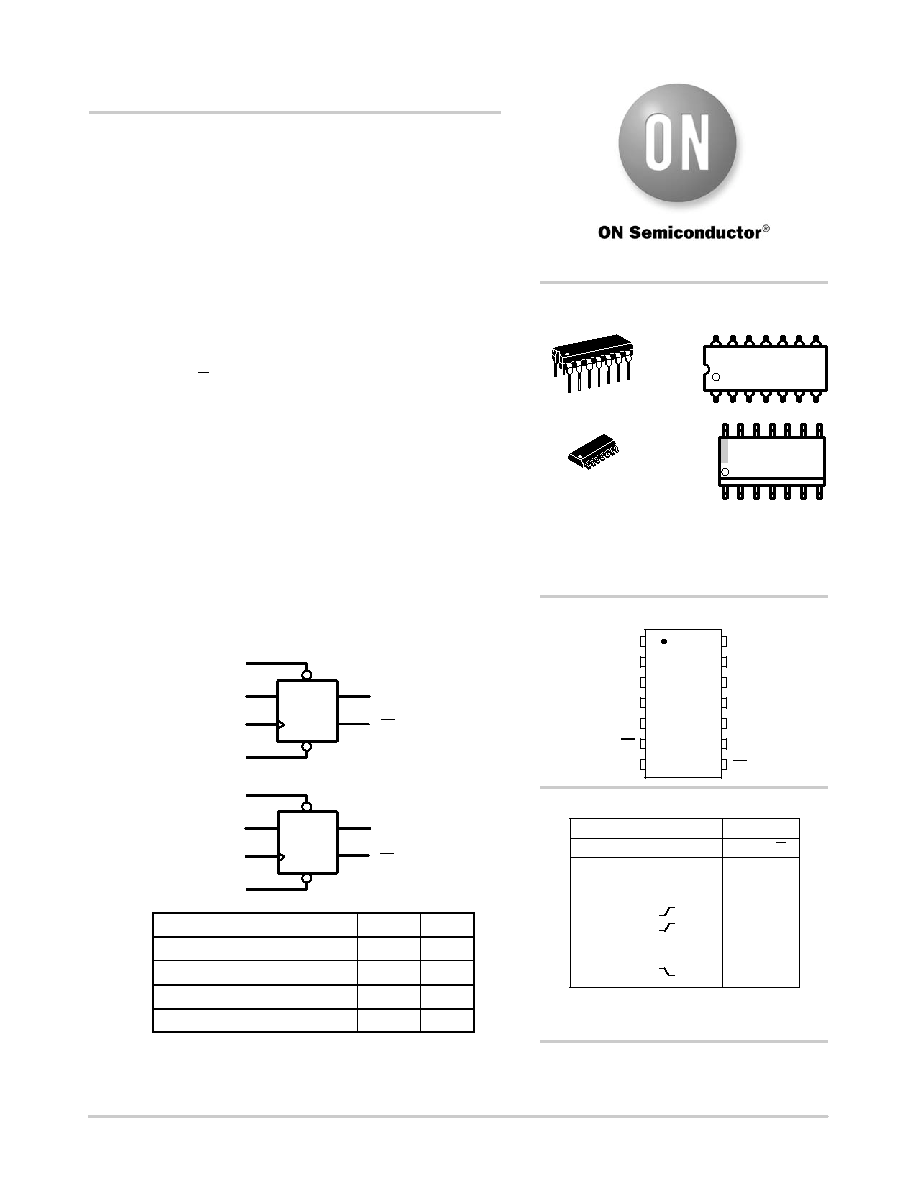
LOGIC DIAGRAM
RESET 1
DATA 1
CLOCK 1
SET 1
RESET 2
DATA 2
CLOCK 2
SET 2
1
2
3
4
13
12
11
10
5
6
9
8
Q1
Q2
PIN 14 = VCC
PIN 7 = GND
Design Criteria
Value
Units
Internal Gate Count
34
ea.
Internal Gate Propagation Delay
1.5
ns
Internal Gate Power Dissipation
5.0
mW
Speed Power Product
.0075
pJ
Equivalent to a twoinput NAND gate.
http://onsemi.com
MARKING
DIAGRAMS
A
= Assembly Location
L, WL
= Wafer Lot
Y, YY
= Year
W, WW = Work Week
G= PbFree Package
SOIC14
D SUFFIX
CASE 751A
14
1
HCT74AG
AWLYWW
1
14
1
PDIP14
N SUFFIX
CASE 646
MC74HCT74AN
AWLYYWWG
1
14
See detailed ordering and shipping information in the package
dimensions section on page 3 of this data sheet.
ORDERING INFORMATION
PIN ASSIGNMENT
SET 1
CLOCK 1
DATA 1
RESET 1
11
12
13
14
8
9
10
5
4
3
2
1
7
6
SET 2
CLOCK 2
DATA 2
RESET 2
VCC
Q2
GND
Q1
FUNCTION TABLE
Inputs
Outputs
Set Reset Clock Data
Q
LH
X
HL
X
L
H
L
X
H*
HH
H
L
HH
L
H
L
X
No Change
H
X
No Change
H
X
No Change
*Both outputs will remain high as long as Set and
Reset are low, but the output states are unpredict-
able if Set and Reset go high simultaneously.
相关PDF资料 |
PDF描述 |
|---|---|
| NC7SZ374P6X | IC FLIP FLOP DTYPE TRI-ST SC70-6 |
| IDT74FCT521CTPYG | IC COMPARATOR IDENTITY 8B 20SSOP |
| SY10E166JC | IC COMPARATOR MAGNITUDE 28PLCC |
| SY100E166JC | IC COMPARATOR MAGNITUDE 28PLCC |
| M85049/31-8W | E NUT SHELL SIZE 8 CADMIUM |
相关代理商/技术参数 |
参数描述 |
|---|---|
| MC74HCT74ADT | 制造商:Rochester Electronics LLC 功能描述:- Tape and Reel |
| MC74HCT74AN | 功能描述:触发器 5V CMOS Dual D-Type RoHS:否 制造商:Texas Instruments 电路数量:2 逻辑系列:SN74 逻辑类型:D-Type Flip-Flop 极性:Inverting, Non-Inverting 输入类型:CMOS 输出类型: 传播延迟时间:4.4 ns 高电平输出电流:- 16 mA 低电平输出电流:16 mA 电源电压-最大:5.5 V 最大工作温度:+ 85 C 安装风格:SMD/SMT 封装 / 箱体:X2SON-8 封装:Reel |
| MC74HCT74AND | 制造商:Motorola Inc 功能描述: |
| MC74HCT74ANG | 功能描述:触发器 5V CMOS Dual D-Type w/Set Reset RoHS:否 制造商:Texas Instruments 电路数量:2 逻辑系列:SN74 逻辑类型:D-Type Flip-Flop 极性:Inverting, Non-Inverting 输入类型:CMOS 输出类型: 传播延迟时间:4.4 ns 高电平输出电流:- 16 mA 低电平输出电流:16 mA 电源电压-最大:5.5 V 最大工作温度:+ 85 C 安装风格:SMD/SMT 封装 / 箱体:X2SON-8 封装:Reel |
| MC74HCT86ADG | 功能描述:逻辑门 IC QUAD 2-IN EX-OR GATE RoHS:否 制造商:Texas Instruments 产品:OR 逻辑系列:LVC 栅极数量:2 线路数量(输入/输出):2 / 1 高电平输出电流:- 16 mA 低电平输出电流:16 mA 传播延迟时间:3.8 ns 电源电压-最大:5.5 V 电源电压-最小:1.65 V 最大工作温度:+ 125 C 安装风格:SMD/SMT 封装 / 箱体:DCU-8 封装:Reel |
发布紧急采购,3分钟左右您将得到回复。