- 您现在的位置:买卖IC网 > PDF目录25622 > MC74LCX16652DT (ON SEMICONDUCTOR) LVC/LCX/Z SERIES, DUAL 8-BIT REGISTERED TRANSCEIVER, TRUE OUTPUT, PDSO56 PDF资料下载
参数资料
| 型号: | MC74LCX16652DT |
| 厂商: | ON SEMICONDUCTOR |
| 元件分类: | 总线收发器 |
| 英文描述: | LVC/LCX/Z SERIES, DUAL 8-BIT REGISTERED TRANSCEIVER, TRUE OUTPUT, PDSO56 |
| 封装: | PLASTIC, TSSOP-56 |
| 文件页数: | 17/21页 |
| 文件大小: | 544K |
| 代理商: | MC74LCX16652DT |
MC74LCX16652
LCX DATA
BR1339 — REV 3
219
MOTOROLA
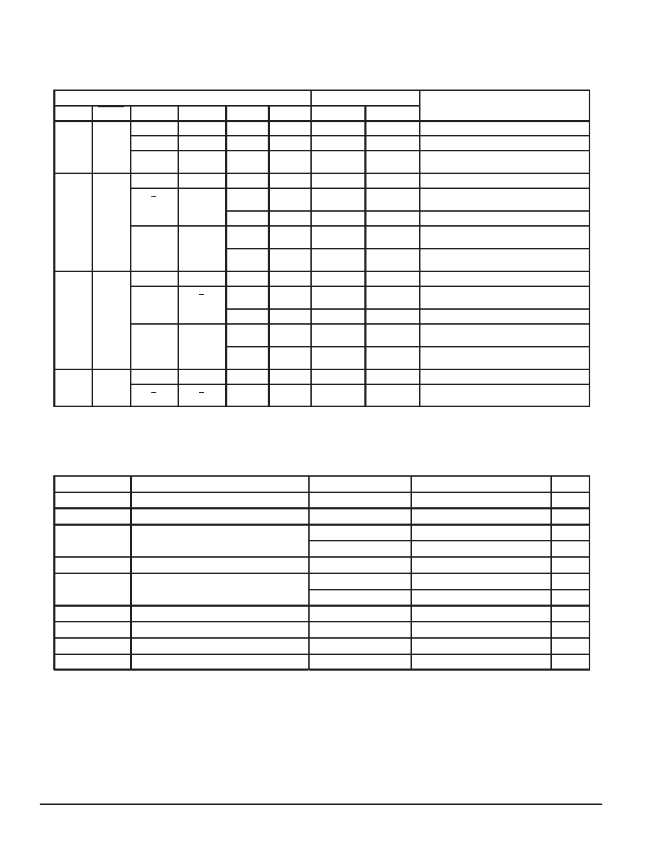
FUNCTION TABLE
Inputs
Data Ports
Operating Mode
OEABn
OEBAn
CABn
CBAn
SABn
SBAn
An
Bn
Operating Mode
L
H
Input
↑
X
Isolation, Hold Storage
↑
X
l
h
l
h
Store A and/or B Data
H
Input
Output
↑
X*
L
X
L
H
L
H
Real Time A Data to B Bus
H
X
QA
Stored A Data to B Bus
↑
X*
L
X
l
h
L
H
Real TIme A Data to B Bus; Store A Data
H
X
L
H
QA
Clock A Data to B Bus; Store A Data
L
Output
Input
X*
↑
X
L
H
L
H
Real Time B Data to A Bus
X
H
QB
X
Stored B Data to A Bus
X*
↑
X
L
H
l
h
Real Time B Data to A Bus; Store B Data
X
H
QB
L
H
Clock B Data to A Bus; Store B Data
H
L
Output
↑
H
QB
QA
Stored A Data to B Bus,
Stored B Data to A Bus
H = High Voltage Level; h = High Voltage Level One Setup Time Prior to the Low–to–High Clock Transition; L = Low Voltage Level; l = Low Voltage Level One Setup
Time Prior to the Low–to–High Clock Transition; X = Don’t Care;
↑ = Low–to–High Clock Transition; ↑ = NOT Low–to–High Clock Transition; QA = A input storage register;
QB = B input storage register; * = The clocks are not internally gated with either the Output Enables or the Source Inputs. Therefore, data at the A or B ports may be
clocked into the storage registers, at any time. For ICC reasons, Do Not Float Inputs.
ABSOLUTE MAXIMUM RATINGS*
Symbol
Parameter
Value
Condition
Unit
VCC
DC Supply Voltage
–0.5 to +7.0
V
VI
DC Input Voltage
–0.5
≤ VI ≤ +7.0
V
VO
DC Output Voltage
–0.5
≤ VO ≤ +7.0
Output in 3–State
V
–0.5
≤ VO ≤ VCC + 0.5
Note 1.
V
IIK
DC Input Diode Current
–50
VI < GND
mA
IOK
DC Output Diode Current
–50
VO < GND
mA
+50
VO > VCC
mA
IO
DC Output Source/Sink Current
±50
mA
ICC
DC Supply Current Per Supply Pin
±100
mA
IGND
DC Ground Current Per Ground Pin
±100
mA
TSTG
Storage Temperature Range
–65 to +150
°C
* Absolute maximum continuous ratings are those values beyond which damage to the device may occur. Exposure to these conditions or conditions
beyond those indicated may adversely affect device reliability. Functional operation under absolute–maximum–rated conditions is not implied.
1. Output in HIGH or LOW State. IO absolute maximum rating must be observed.
相关PDF资料 |
PDF描述 |
|---|---|
| MC74LCX244DWR2 | LVC/LCX/Z SERIES, DUAL 4-BIT DRIVER, TRUE OUTPUT, PDSO20 |
| MC74LCX74SDR2 | LVC/LCX/Z SERIES, DUAL POSITIVE EDGE TRIGGERED D FLIP-FLOP, COMPLEMENTARY OUTPUT, PDSO14 |
| MC74LVX244DTR2 | LV/LV-A/LVX/H SERIES, DUAL 4-BIT DRIVER, TRUE OUTPUT, PDSO20 |
| MC74LVX595M | LV/LV-A/LVX/H SERIES, 8-BIT RIGHT SERIAL IN PARALLEL OUT SHIFT REGISTER, TRUE OUTPUT, PDSO16 |
| MC74VCX16240DT | ALVC/VCX/A SERIES, QUAD 4-BIT DRIVER, INVERTED OUTPUT, PDSO48 |
相关代理商/技术参数 |
参数描述 |
|---|---|
| MC74LCX240D | 制造商:ON Semiconductor 功能描述: |
| MC74LCX240DT | 制造商:Rochester Electronics LLC 功能描述:- Tape and Reel |
| MC74LCX240DTR2 | 功能描述:缓冲器和线路驱动器 2-36.V Octal 3-State RoHS:否 制造商:Micrel 输入线路数量:1 输出线路数量:2 极性:Non-Inverting 电源电压-最大:+/- 5.5 V 电源电压-最小:+/- 2.37 V 最大工作温度:+ 85 C 安装风格:SMD/SMT 封装 / 箱体:MSOP-8 封装:Reel |
| MC74LCX240DTR2G | 功能描述:缓冲器和线路驱动器 2-36.V Octal 3-State Inverting RoHS:否 制造商:Micrel 输入线路数量:1 输出线路数量:2 极性:Non-Inverting 电源电压-最大:+/- 5.5 V 电源电压-最小:+/- 2.37 V 最大工作温度:+ 85 C 安装风格:SMD/SMT 封装 / 箱体:MSOP-8 封装:Reel |
| MC74LCX240DWR2 | 功能描述:缓冲器和线路驱动器 2-36.V Octal 3-State RoHS:否 制造商:Micrel 输入线路数量:1 输出线路数量:2 极性:Non-Inverting 电源电压-最大:+/- 5.5 V 电源电压-最小:+/- 2.37 V 最大工作温度:+ 85 C 安装风格:SMD/SMT 封装 / 箱体:MSOP-8 封装:Reel |
发布紧急采购,3分钟左右您将得到回复。