参数资料
| 型号: | MC74LVX4052MELG |
| 厂商: | ON Semiconductor |
| 文件页数: | 3/15页 |
| 文件大小: | 0K |
| 描述: | IC MUX/DEMUX DUAL 4X1 16SOEIAJ |
| 产品变化通告: | Product Discontinuation 30/Sept/2011 |
| 标准包装: | 1 |
| 系列: | 74LVX |
| 功能: | 多路复用器/多路分解器 |
| 电路: | 2 x 4:1 |
| 导通状态电阻: | 55 欧姆 |
| 电压电源: | 单电源 |
| 电压 - 电源,单路/双路(±): | 2.5 V ~ 6 V |
| 电流 - 电源: | 40µA |
| 工作温度: | -55°C ~ 125°C |
| 安装类型: | 表面贴装 |
| 封装/外壳: | 16-SOIC(0.209",5.30mm 宽) |
| 供应商设备封装: | 16-SOEIAJ |
| 包装: | 剪切带 (CT) |
| 其它名称: | MC74LVX4052MELGOSCT |
MC74LVX4052
http://onsemi.com
11
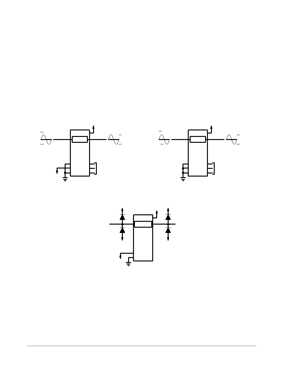
APPLICATIONS INFORMATION
The Channel Select and Enable control pins should be at
VCC or GND logic levels. VCC being recognized as a logic
high and GND being recognized as a logic low. In this
example:
VCC = )5 V = logic high
GND = 0 V = logic low
The maximum analog voltage swing is determined by the
supply voltages VCC and VEE. The positive peak analog
voltage should not exceed VCC. Similarly, the negative peak
analog voltage should not go below VEE. In this example,
the difference between VCC and VEE is 5.0 volts. Therefore,
using the configuration of Figure 21, a maximum analog
signal of 5.0 volts peaktopeak can be controlled. Unused
analog inputs/outputs may be left floating (i.e., not
connected). However, tying unused analog inputs and
outputs to VCC or GND through a low value resistor helps
minimize crosstalk and feedthrough noise that may be
picked up by an unused switch.
Although used here, balanced supplies are not a
requirement. The only constraints on the power supplies are
that:
VEE GND = 0 to *6 volts
VCC GND = 2.5 to 6 volts
VCC VEE = 2.5 to 6 volts
and VEE v GND
When voltage transients above VCC and/or below VEE are
anticipated on the analog channels, external Germanium or
Schottky diodes (Dx) are recommended as shown in
Figure 22. These diodes should be able to absorb the
maximum anticipated current surges during clipping.
ANALOG
SIGNAL
Figure 20. Application Example
ON
6
7
8
16
+3.0 V
ANALOG
SIGNAL
+3.0 V
3.0 V
+3.0 V
3.0 V
11
10
9
TO EXTERNAL CMOS
CIRCUITRY 0 to 3.0 V
DIGITAL SIGNALS
3.0 V
Figure 21. Application Example
ANALOG
SIGNAL
ON
6
7
8
16
+5 V
ANALOG
SIGNAL
+5 V
GND
+5 V
GND
11
10
9
TO EXTERNAL CMOS
CIRCUITRY 0 to 5 V
DIGITAL SIGNALS
ON/OFF
7
8
16
VCC
VEE
Dx
VCC
Dx
VEE
Dx
VCC
Dx
VEE
Figure 22. External Germanium or Schottky Clipping Diodes
相关PDF资料 |
PDF描述 |
|---|---|
| MC74LVX4053MG | IC MUX/DEMUX TRIPLE 2X1 16SOEIAJ |
| MC74LVX4066MELG | IC MUX/DEMUX QUAD 1X1 14SOEIAJ |
| MC74LVX8051MG | IC MUX/DEMUX 8X1 16SOEIAJ |
| MC74LVX8053MELG | IC MUX/DEMUX TRIPLE 2X1 16SOEIAJ |
| MC74LVXT4051MELG | IC MUX/DEMUX 8X1 16SOEIAJ |
相关代理商/技术参数 |
参数描述 |
|---|---|
| MC74LVX4052MG | 功能描述:多路器开关 IC 2.5-6V Analog Mux/DeMux RoHS:否 制造商:Texas Instruments 通道数量:1 开关数量:4 开启电阻(最大值):7 Ohms 开启时间(最大值): 关闭时间(最大值): 传播延迟时间:0.25 ns 工作电源电压:2.3 V to 3.6 V 工作电源电流: 最大工作温度:+ 85 C 安装风格:SMD/SMT 封装 / 箱体:UQFN-16 |
| MC74LVX4053D | 功能描述:多路器开关 IC 2.5-6V Analog RoHS:否 制造商:Texas Instruments 通道数量:1 开关数量:4 开启电阻(最大值):7 Ohms 开启时间(最大值): 关闭时间(最大值): 传播延迟时间:0.25 ns 工作电源电压:2.3 V to 3.6 V 工作电源电流: 最大工作温度:+ 85 C 安装风格:SMD/SMT 封装 / 箱体:UQFN-16 |
| MC74LVX4053DG | 功能描述:多路器开关 IC 2.5-6V Analog Mux/DeMux RoHS:否 制造商:Texas Instruments 通道数量:1 开关数量:4 开启电阻(最大值):7 Ohms 开启时间(最大值): 关闭时间(最大值): 传播延迟时间:0.25 ns 工作电源电压:2.3 V to 3.6 V 工作电源电流: 最大工作温度:+ 85 C 安装风格:SMD/SMT 封装 / 箱体:UQFN-16 |
| MC74LVX4053DR2 | 功能描述:多路器开关 IC LOG CMOS MLTIPLXR RoHS:否 制造商:Texas Instruments 通道数量:1 开关数量:4 开启电阻(最大值):7 Ohms 开启时间(最大值): 关闭时间(最大值): 传播延迟时间:0.25 ns 工作电源电压:2.3 V to 3.6 V 工作电源电流: 最大工作温度:+ 85 C 安装风格:SMD/SMT 封装 / 箱体:UQFN-16 |
| MC74LVX4053DR2G | 功能描述:多路器开关 IC 2.5-6V Analog Mux/DeMux RoHS:否 制造商:Texas Instruments 通道数量:1 开关数量:4 开启电阻(最大值):7 Ohms 开启时间(最大值): 关闭时间(最大值): 传播延迟时间:0.25 ns 工作电源电压:2.3 V to 3.6 V 工作电源电流: 最大工作温度:+ 85 C 安装风格:SMD/SMT 封装 / 箱体:UQFN-16 |
发布紧急采购,3分钟左右您将得到回复。