- 您现在的位置:买卖IC网 > PDF目录11064 > MC74LVX8053DR2 (ON Semiconductor)IC MUX/DEMUX TRIPLE 2X1 16SOIC PDF资料下载
参数资料
| 型号: | MC74LVX8053DR2 |
| 厂商: | ON Semiconductor |
| 文件页数: | 8/14页 |
| 文件大小: | 0K |
| 描述: | IC MUX/DEMUX TRIPLE 2X1 16SOIC |
| 产品变化通告: | Product Obsolescence 11/Feb/2009 |
| 标准包装: | 2,500 |
| 系列: | 74LVX |
| 功能: | 多路复用器/多路分解器 |
| 电路: | 3 x 2:1 |
| 导通状态电阻: | 30 欧姆 |
| 电压电源: | 单电源 |
| 电压 - 电源,单路/双路(±): | 2 V ~ 6 V |
| 电流 - 电源: | 40µA |
| 工作温度: | -55°C ~ 85°C |
| 安装类型: | 表面贴装 |
| 封装/外壳: | 16-SOIC(0.154",3.90mm 宽) |
| 供应商设备封装: | 16-SOIC |
| 包装: | 带卷 (TR) |
MC74LVX8053
http://onsemi.com
3
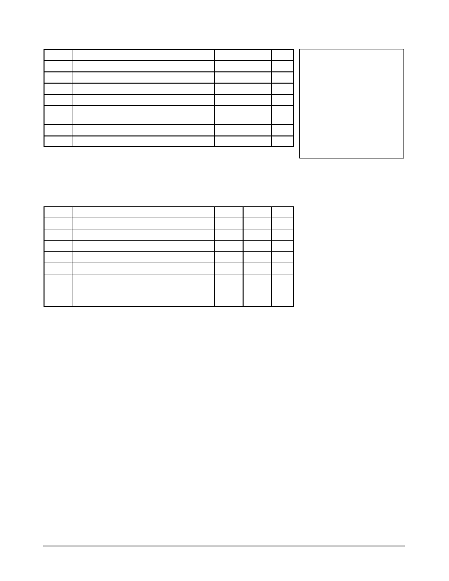
MAXIMUM RATINGS
Symbol
Parameter
Value
Unit
VCC
Positive DC Supply Voltage
(Referenced to GND)
– 0.5 to + 7.0
V
VIS
Analog Input Voltage
0.5 to VCC + 0.5
V
Vin
Digital Input Voltage (Referenced to GND)
– 0.5 to VCC + 0.5
V
I
DC Current, Into or Out of Any Pin
± 20
mA
PD
Power Dissipation in Still Air,
SOIC Package
TSSOP Package
500
450
mW
Tstg
Storage Temperature Range
– 65 to + 150
_C
TL
Lead Temperature, 1 mm from Case for 10 Seconds
260
_C
Maximum ratings are those values beyond which device damage can occur. Maximum ratings
applied to the device are individual stress limit values (not normal operating conditions) and are
not valid simultaneously. If these limits are exceeded, device functional operation is not implied,
damage may occur and reliability may be affected.
Derating — SOIC Package: – 7 mW/_C from 65_ to 125_C
TSSOP Package: 6.1 mW/_C from 65_ to 125_C
RECOMMENDED OPERATING CONDITIONS
Symbol
Parameter
Min
Max
Unit
VCC
Positive DC Supply Voltage
(Referenced to GND)
2.5
6.0
V
VIS
Analog Input Voltage
0.0
VCC
V
Vin
Digital Input Voltage (Referenced to GND)
GND
VCC
V
VIO*
Static or Dynamic Voltage Across Switch
1.2
V
TA
Operating Temperature Range, All Package Types
– 55
+ 85
_C
tr, tf
Input Rise/Fall Time
(Channel Select or Enable Inputs)
VCC = 3.3 V ± 0.3 V
VCC = 5.0 V ± 0.5 V
0
100
20
ns/V
*For voltage drops across switch greater than 1.2 V (switch on), excessive VCC current may be
drawn; i.e., the current out of the switch may contain both VCC and switch input components. The
reliability of the device will be unaffected unless the Maximum Ratings are exceeded.
This device contains protection
circuitry to guard against damage
due to high static voltages or electric
fields. However, precautions must
be taken to avoid applications of any
voltage higher than maximum rated
voltages to this highimpedance cir-
cuit. For proper operation, Vin and
Vout should be constrained to the
range GND v (Vin or Vout) v VCC.
Unused inputs must always be
tied to an appropriate logic voltage
level (e.g., either GND or VCC).
Unused outputs must be left open.
相关PDF资料 |
PDF描述 |
|---|---|
| MC74LVX8051MELG | IC MUX/DEMUX 8X1 16SOEIAJ |
| MC74LVX8051MEL | IC MUX/DEMUX 8X1 16SOEIAJ |
| MC74LVX8051M | IC MUX/DEMUX 8X1 16SOEIAJ |
| MC74LVX8051DTR2 | IC MUX/DEMUX 8X1 16TSSOP |
| DF36034FPV | IC H8/36034 MCU FLASH 64LQFP |
相关代理商/技术参数 |
参数描述 |
|---|---|
| MC74LVX8053DR2G | 功能描述:多路器开关 IC 2-6V ANLG Mux/Demux -55 to 85deg C RoHS:否 制造商:Texas Instruments 通道数量:1 开关数量:4 开启电阻(最大值):7 Ohms 开启时间(最大值): 关闭时间(最大值): 传播延迟时间:0.25 ns 工作电源电压:2.3 V to 3.6 V 工作电源电流: 最大工作温度:+ 85 C 安装风格:SMD/SMT 封装 / 箱体:UQFN-16 |
| MC74LVX8053DT | 制造商:Rochester Electronics LLC 功能描述:- Bulk |
| MC74LVX8053DTR2 | 功能描述:多路器开关 IC 2-6V ANLG Mux/Demux RoHS:否 制造商:Texas Instruments 通道数量:1 开关数量:4 开启电阻(最大值):7 Ohms 开启时间(最大值): 关闭时间(最大值): 传播延迟时间:0.25 ns 工作电源电压:2.3 V to 3.6 V 工作电源电流: 最大工作温度:+ 85 C 安装风格:SMD/SMT 封装 / 箱体:UQFN-16 |
| MC74LVX8053DTR2G | 功能描述:多路器开关 IC 2-6V ANLG Mux/Demux -55 to 85deg C RoHS:否 制造商:Texas Instruments 通道数量:1 开关数量:4 开启电阻(最大值):7 Ohms 开启时间(最大值): 关闭时间(最大值): 传播延迟时间:0.25 ns 工作电源电压:2.3 V to 3.6 V 工作电源电流: 最大工作温度:+ 85 C 安装风格:SMD/SMT 封装 / 箱体:UQFN-16 |
| MC74LVX8053M | 功能描述:多路器开关 IC 2-6V ANLG Mux/Demux RoHS:否 制造商:Texas Instruments 通道数量:1 开关数量:4 开启电阻(最大值):7 Ohms 开启时间(最大值): 关闭时间(最大值): 传播延迟时间:0.25 ns 工作电源电压:2.3 V to 3.6 V 工作电源电流: 最大工作温度:+ 85 C 安装风格:SMD/SMT 封装 / 箱体:UQFN-16 |
发布紧急采购,3分钟左右您将得到回复。