- 您现在的位置:买卖IC网 > PDF目录25622 > MC74VHC1GT86DTT3 (ON SEMICONDUCTOR) AHC/VHC SERIES, 2-INPUT XOR GATE, PDSO5 PDF资料下载
参数资料
| 型号: | MC74VHC1GT86DTT3 |
| 厂商: | ON SEMICONDUCTOR |
| 元件分类: | 门电路 |
| 英文描述: | AHC/VHC SERIES, 2-INPUT XOR GATE, PDSO5 |
| 封装: | SC-59, SOT-23, TSOP-5 |
| 文件页数: | 1/12页 |
| 文件大小: | 122K |
| 代理商: | MC74VHC1GT86DTT3 |
Semiconductor Components Industries, LLC, 2001
April, 2001 – Rev. 7
1
Publication Order Number:
MC74VHC1GT86/D
MC74VHC1GT86
2-Input Exclusive OR Gate /
CMOS Logic Level Shifter
with LSTTL–Compatible Inputs
The MC74VHC1GT86 is an advanced high speed CMOS 2–input
Exclusive OR gate fabricated with silicon gate CMOS technology. It
achieves high speed operation similar to equivalent Bipolar Schottky
TTL while maintaining CMOS low power dissipation.
The internal circuit is composed of three stages, including a buffer
output which provides high noise immunity and stable output.
The device input is compatible with TTL–type input thresholds and the
output has a full 5 V CMOS level output swing. The input protection
circuitry on this device allows overvoltage tolerance on the input,
allowing the device to be used as a logic–level translator from 3.0 V
CMOS logic to 5.0V CMOS Logic or from 1.8 V CMOS logic to 3.0 V
CMOS Logic while operating at the high–voltage power supply.
The MC74VHC1GT86 input structure provides protection when
voltages up to 7 V are applied, regardless of the supply voltage. This
allows the MC74VHC1GT86 to be used to interface 5 V circuits to 3 V
circuits. The output structures also provide protection when VCC = 0 V.
These input and output structures help prevent device destruction caused
by supply voltage – input/output voltage mismatch, battery backup, hot
insertion, etc.
High Speed: t
PD = 4.8 ns (Typ) at VCC = 5 V
Low Power Dissipation: I
CC = 2 A (Max) at TA = 25°C
TTL–Compatible Inputs: V
IL = 0.8 V; VIH = 2.0 V
CMOS–Compatible Outputs: V
OH > 0.8 VCC; VOL < 0.1 VCC @Load
Power Down Protection Provided on Inputs and Outputs
Balanced Propagation Delays
Pin and Function Compatible with Other Standard Logic Families
Chip Complexity: FETs = 83; Equivalent Gates = 16
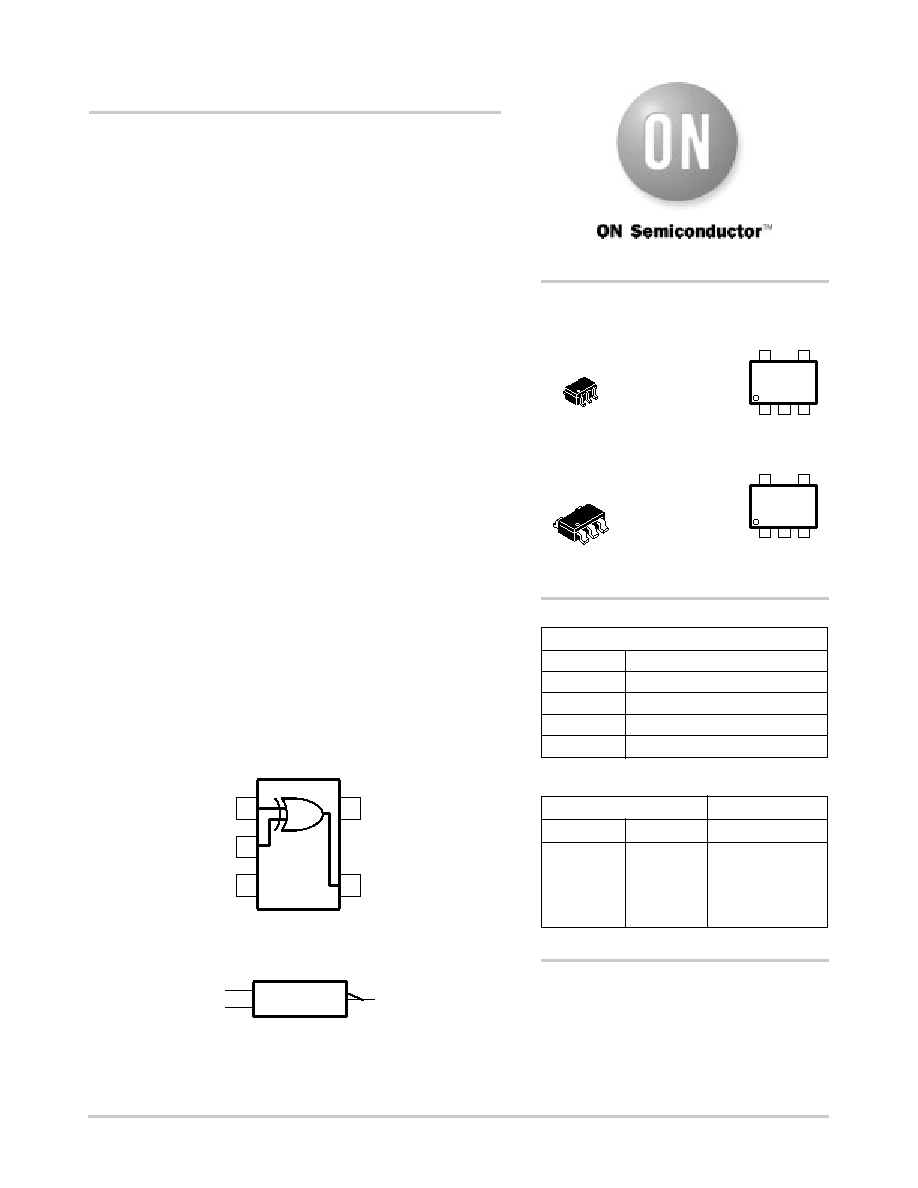
Figure 1. Pinout (Top View)
IN A
OUT Y
= 1
IN B
VCC
IN B
IN A
OUT Y
GND
Figure 2. Logic Symbol
1
2
3
4
5
PIN ASSIGNMENT
1
2
3
GND
IN B
IN A
http://onsemi.com
4
5VCC
OUT Y
L
H
L
H
L
H
FUNCTION TABLE
Inputs
Output
AB
L
H
L
Y
See detailed ordering and shipping information in the package
dimensions section on page 4 of this data sheet.
ORDERING INFORMATION
SC–88A / SOT–353/SC–70
DF SUFFIX
CASE 419A
Pin 1
d = Date Code
VMd
TSOP–5/SOT–23/SC–59
DT SUFFIX
CASE 483
Pin 1
d = Date Code
VMd
MARKING
DIAGRAMS
相关PDF资料 |
PDF描述 |
|---|---|
| MC74VHCT374ADWR2G | AHCT/VHCT SERIES, 8-BIT DRIVER, TRUE OUTPUT, PDSO20 |
| MC80C32-16/883 | 8-BIT, 16 MHz, MICROCONTROLLER, CDIP40 |
| MR80C52XXX-16P883D | 8-BIT, MROM, 16 MHz, MICROCONTROLLER, CQCC44 |
| MR80C32-25/883 | 8-BIT, 25 MHz, MICROCONTROLLER, CQCC44 |
| MEGA32C1-15AZ | 8-BIT, FLASH, 16 MHz, RISC MICROCONTROLLER, PQFP32 |
相关代理商/技术参数 |
参数描述 |
|---|---|
| MC74VHC1GU04DF1G | 功能描述:变换器 LOG CMOS INVERTER GATE RoHS:否 制造商:NXP Semiconductors 电路数量:6 逻辑系列:74ABT 逻辑类型:BiCMOS 高电平输出电流:- 15 mA 低电平输出电流:20 mA 传播延迟时间:2.2 ns 电源电压-最大:5.5 V 电源电压-最小:4.5 V 最大工作温度:+ 85 C 最小工作温度:- 40 C 工作温度范围: 封装 / 箱体:DIP-14 封装:Tube |
| MC74VHC1GU04DF2G | 制造商:Rochester Electronics LLC 功能描述:- Bulk |
| MC74VHC1GU04DFT1 | 功能描述:变换器 2-5.5V CMOS Single RoHS:否 制造商:NXP Semiconductors 电路数量:6 逻辑系列:74ABT 逻辑类型:BiCMOS 高电平输出电流:- 15 mA 低电平输出电流:20 mA 传播延迟时间:2.2 ns 电源电压-最大:5.5 V 电源电压-最小:4.5 V 最大工作温度:+ 85 C 最小工作温度:- 40 C 工作温度范围: 封装 / 箱体:DIP-14 封装:Tube |
| MC74VHC1GU04DFT2 | 功能描述:变换器 2-5.5V CMOS Single RoHS:否 制造商:NXP Semiconductors 电路数量:6 逻辑系列:74ABT 逻辑类型:BiCMOS 高电平输出电流:- 15 mA 低电平输出电流:20 mA 传播延迟时间:2.2 ns 电源电压-最大:5.5 V 电源电压-最小:4.5 V 最大工作温度:+ 85 C 最小工作温度:- 40 C 工作温度范围: 封装 / 箱体:DIP-14 封装:Tube |
| MC74VHC1GU04DFTG | 制造商:ON Semiconductor 功能描述:Inverter 1-Element CMOS 5-Pin SC-70 T/R |
发布紧急采购,3分钟左右您将得到回复。