- 您现在的位置:买卖IC网 > PDF目录11199 > MC74VHC4066DTR2G (ON Semiconductor)IC MUX/DEMUX QUAD 1X1 14TSSOP PDF资料下载
参数资料
| 型号: | MC74VHC4066DTR2G |
| 厂商: | ON Semiconductor |
| 文件页数: | 2/14页 |
| 文件大小: | 0K |
| 描述: | IC MUX/DEMUX QUAD 1X1 14TSSOP |
| 标准包装: | 2,500 |
| 系列: | 74VHC |
| 功能: | 多路复用器/多路分解器 |
| 电路: | 4 x 1:1 |
| 导通状态电阻: | 85 欧姆 |
| 电压电源: | 单电源 |
| 电压 - 电源,单路/双路(±): | 2 V ~ 12 V |
| 电流 - 电源: | 40µA |
| 工作温度: | -55°C ~ 125°C |
| 安装类型: | 表面贴装 |
| 封装/外壳: | 14-TSSOP(0.173",4.40mm 宽) |
| 供应商设备封装: | 14-TSSOP |
| 包装: | 带卷 (TR) |
MC74VHC4066
http://onsemi.com
10
0
-10
-20
-30
-40
-50
1.0
2.0
FREQUENCY (kHz)
dBm
-60
-70
-80
-90
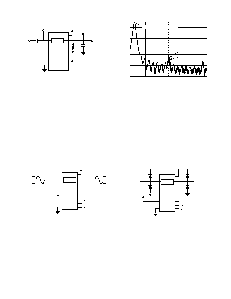
FUNDAMENTAL FREQUENCY
DEVICE
SOURCE
Figure 19. Plot, Harmonic Distortion
3.0
ON
VCC
0.1
μF
CL*
fin
RL
TO
DISTORTION
METER
*Includes all probe and jig capacitance.
VOS
VIS
7
SELECTED
CONTROL
INPUT
VCC
Figure 20. Total Harmonic Distortion, Test SetUp
VCC/2
APPLICATION INFORMATION
The ON/OFF Control pins should be at VCC or GND logic
levels, VCC being recognized as logic high and GND being
recognized as a logic low. Unused analog inputs/outputs
may be left floating (not connected). However, it is
advisable to tie unused analog inputs and outputs to VCC or
GND through a low value resistor. This minimizes crosstalk
and feedthrough noise that may be pickedup by the
unused I/O pins.
The maximum analog voltage swings are determined by
the supply voltages VCC and GND. The positive peak
analog voltage should not exceed VCC. Similarly, the
negative peak analog voltage should not go below GND. In
the example below, the difference between VCC and GND is
twelve volts. Therefore, using the configuration in Figure 21,
a maximum analog signal of twelve volts peaktopeak can
be controlled.
When voltage transients above VCC and/or below GND
are anticipated on the analog channels, external diodes
(Dx) are recommended as shown in Figure 22. These
diodes should be small signal, fast turnon types able to
absorb the maximum anticipated current surges during
clipping. An alternate method would be to replace the Dx
diodes with Mosorbs (high current surge protectors).
Mosorbs are fast turnon devices ideally suited for precise
DC protection with no inherent wear out mechanism.
ANALOG O/I
ON
14
VCC = 12 V
ANALOG I/O
+ 12 V
0 V
+ 12 V
0 V
OTHER CONTROL
INPUTS
(VCC OR GND)
ON
16
VCC
Dx
VCC
Dx
Figure 21. 12 V Application
Figure 22. Transient Suppressor Application
7
SELECTED
CONTROL
INPUT
Dx
OTHER CONTROL
INPUTS
(VCC OR GND)
7
SELECTED
CONTROL
INPUT
VCC
相关PDF资料 |
PDF描述 |
|---|---|
| VI-B4R-IX-F2 | CONVERTER MOD DC/DC 7.5V 75W |
| MC74VHC4066DR2G | IC MUX/DEMUX QUAD 1X1 16SOIC |
| VI-B4R-IX | CONVERTER MOD DC/DC 7.5V 75W |
| MC74VHC4053DR2G | IC MUX/DEMUX TRIPLE 2X1 16SOIC |
| FSA4157P6X | IC SWITCH SPDT SC70-6 |
相关代理商/技术参数 |
参数描述 |
|---|---|
| MC74VHC4066M | 功能描述:模拟开关 IC 2-12V ANLG Mux/Demux RoHS:否 制造商:Texas Instruments 开关数量:2 开关配置:SPDT 开启电阻(最大值):0.1 Ohms 切换电压(最大): 开启时间(最大值): 关闭时间(最大值): 工作电源电压:2.7 V to 4.5 V 最大工作温度:+ 85 C 安装风格:SMD/SMT 封装 / 箱体:DSBGA-16 |
| MC74VHC4066MEL | 功能描述:模拟开关 IC 2-12V ANLG Mux/Demux RoHS:否 制造商:Texas Instruments 开关数量:2 开关配置:SPDT 开启电阻(最大值):0.1 Ohms 切换电压(最大): 开启时间(最大值): 关闭时间(最大值): 工作电源电压:2.7 V to 4.5 V 最大工作温度:+ 85 C 安装风格:SMD/SMT 封装 / 箱体:DSBGA-16 |
| MC74VHC4066MELG | 功能描述:多路器开关 IC 2-12V ANLG Mux/Demux -55 to 85deg C RoHS:否 制造商:Texas Instruments 通道数量:1 开关数量:4 开启电阻(最大值):7 Ohms 开启时间(最大值): 关闭时间(最大值): 传播延迟时间:0.25 ns 工作电源电压:2.3 V to 3.6 V 工作电源电流: 最大工作温度:+ 85 C 安装风格:SMD/SMT 封装 / 箱体:UQFN-16 |
| MC74VHC4066MG | 功能描述:多路器开关 IC 2-12V ANLG Mux/Demux -55 to 85deg C RoHS:否 制造商:Texas Instruments 通道数量:1 开关数量:4 开启电阻(最大值):7 Ohms 开启时间(最大值): 关闭时间(最大值): 传播延迟时间:0.25 ns 工作电源电压:2.3 V to 3.6 V 工作电源电流: 最大工作温度:+ 85 C 安装风格:SMD/SMT 封装 / 箱体:UQFN-16 |
| MC74VHC4316D | 功能描述:模拟开关 IC LOG CMOS QUAD MX/ DEMX RoHS:否 制造商:Texas Instruments 开关数量:2 开关配置:SPDT 开启电阻(最大值):0.1 Ohms 切换电压(最大): 开启时间(最大值): 关闭时间(最大值): 工作电源电压:2.7 V to 4.5 V 最大工作温度:+ 85 C 安装风格:SMD/SMT 封装 / 箱体:DSBGA-16 |
发布紧急采购,3分钟左右您将得到回复。