参数资料
| 型号: | MC75174BPG |
| 厂商: | ON Semiconductor |
| 文件页数: | 6/13页 |
| 文件大小: | 0K |
| 描述: | IC LINEDRVR QUAD EIA485 16-DIP |
| 产品变化通告: | Product Obsolescence 24/Jan/2011 |
| 标准包装: | 25 |
| 类型: | 线路驱动器,发射器 |
| 驱动器/接收器数: | 4/0 |
| 规程: | RS422,RS485 |
| 电源电压: | 4.75 V ~ 5.25 V |
| 安装类型: | 通孔 |
| 封装/外壳: | 16-DIP(0.300",7.62mm) |
| 供应商设备封装: | 16-DIP |
| 包装: | 管件 |
MC75172B, MC75174B
http://onsemi.com
2
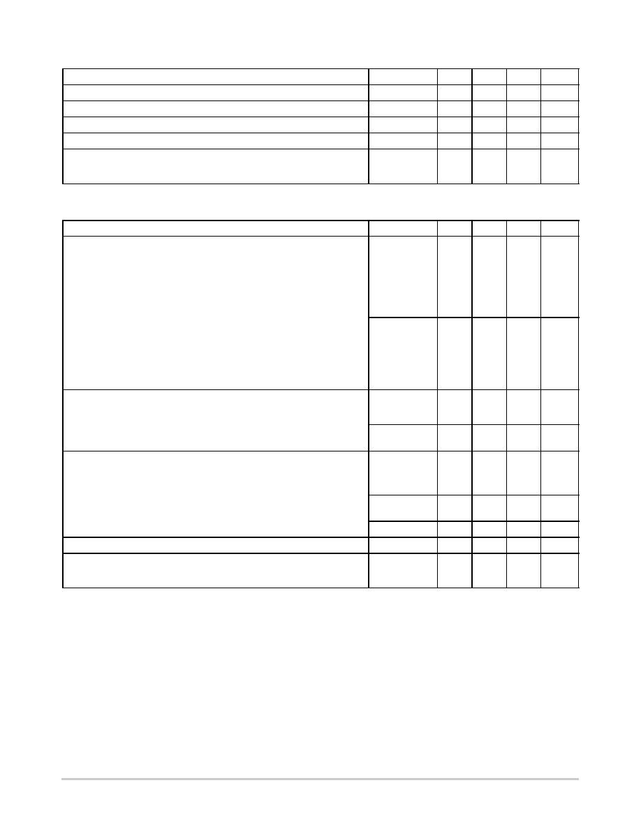
RECOMMENDED OPERATING CONDITIONS
Characteristic
Symbol
Min
Typ
Max
Unit
Power Supply Voltage
VCC
+4.75
+5.0
+5.25
Vdc
Input Voltage (All Inputs)
Vin
0
VCC
Vdc
Output Voltage in 3State Condition, or when VCC = 0 V
Vcm
7.0
+12
Vdc
Output Current (Normal data transmission)
IO
65
+65
mA
Operating Ambient Temperature (see text)
EIA485
EIA422
TA
40
0
+85
°C
2. All limits are not necessarily functional concurrently.
ELECTRICAL CHARACTERISTICS (40
°C p TA p 85°C, 4.75 V p VCC p 5.25 V, unless otherwise noted.)
Characteristic
Symbol
Min
Typ
Max
Unit
Output Voltage
SingleEnded Voltage
IO = 0
High @ IO = 33 mA
Low @ IO = +33 mA
Differential Voltage
Open Circuit (IO = 0)
RL = 54 W (Figure 1)
VO
VOH
VOL
VOD1
VOD2
0
1.5
4.0
1.6
3.4
2.3
6.0
6.0
5.0
Vdc
Change in Differential*, RL = 54 W (Figure 1)
Differential Voltage, RL = 100 W (Figure 1)
Change in Differential*, RL = 100 W (Figure 1)
Differential Voltage, 7.0 V
p Vcm p 12 V (Figure 2)
Change in Differential*, 7.0 V
p Vcm p 12 V (Figure 2)
Offset Voltage, RL = 54 W (Figure 1)
Change in Offset*, RL = 54 W (Figure 1)
DVOD2
VOD2A
DVOD2A
VOD3
DVOD3
VOS
DVOS
1.5
5.0
2.2
5.0
5.0
2.9
5.0
200
200
5.0
200
200
mVdc
Vdc
mVdc
Vdc
mVdc
Vdc
mVdc
Output Current (Each Output)
Power Off Leakage, VCC = 0, 7.0 V p VO p 12 V
Leakage in 3State Mode, 7.0 V
p VO p 12 V
IO(off)
IOZ
50
0
+50
mA
Short Circuit Current to Ground
Short Circuit Current, 7.0 V
p VO p 12 V
IOSR
IOS
150
250
+150
+250
mA
Inputs
Low Level Voltage (Pins 4 & 12, MC75174B only)
Low Level Voltage (All Other Pins)
High Level Voltage (All Inputs)
VIL(A)
VIL(B)
VIH
0
2.0
0.7
0.8
VCC
Vdc
Current @ Vin = 2.7 V (All Inputs)
Current @ Vin = 0.5 V (All Inputs)
IIH
IIL
100
0.2
15
20
mA
Clamp Voltage (All Inputs, Iin = 18 mA)
VIK
1.5
Vdc
Thermal Shutdown Junction Temperature
Tjts
+150
°C
Power Supply Current (Outputs Open, VCC = 5.25 V)
Outputs Enable
Outputs Disabled
ICC
60
30
70
40
mA
3. *Vin switched from 0.8 to 2.0 V. Typical values determined at 25°C ambient and 5.0 V supply.
相关PDF资料 |
PDF描述 |
|---|---|
| MC75174BDWG | IC LINEDRVR QUAD EIA485 20-SOICW |
| VI-B3B-MY-S | CONVERTER MOD DC/DC 95V 50W |
| MC75172BDWG | IC LINEDRIVER QUAD 3ST 20-SOICW |
| VI-B3B-MW-S | CONVERTER MOD DC/DC 95V 100W |
| CY28446LFXCT | IC CLOCK CALISTOGA CK410M 64QFN |
相关代理商/技术参数 |
参数描述 |
|---|---|
| MC7520D | 制造商:POSITRONIC INDUSTRIES, INC. 功能描述: 制造商: 功能描述: 制造商:undefined 功能描述: |
| MC75368P | 制造商:Motorola Inc 功能描述: 制造商:MOTOROLA 功能描述: |
| MC75450P | 制造商:National Semiconductor 功能描述:75450 NSC'93 |
| MC75451P | 制造商:Rochester Electronics LLC 功能描述:- Bulk |
| MC75453P | 制造商:Motorola Inc 功能描述: 制造商:MOTOROLA 功能描述: |
发布紧急采购,3分钟左右您将得到回复。