- 您现在的位置:买卖IC网 > PDF目录10994 > MC908KX2CDWER (Freescale Semiconductor)IC MCU 2K FLASH 4/8MHZ 16-SOICW PDF资料下载
参数资料
| 型号: | MC908KX2CDWER |
| 厂商: | Freescale Semiconductor |
| 文件页数: | 141/210页 |
| 文件大小: | 0K |
| 描述: | IC MCU 2K FLASH 4/8MHZ 16-SOICW |
| 标准包装: | 1,000 |
| 系列: | HC08 |
| 核心处理器: | HC08 |
| 芯体尺寸: | 8-位 |
| 速度: | 8MHz |
| 连通性: | SCI |
| 外围设备: | LVD,POR,PWM |
| 输入/输出数: | 13 |
| 程序存储器容量: | 2KB(2K x 8) |
| 程序存储器类型: | 闪存 |
| RAM 容量: | 192 x 8 |
| 电压 - 电源 (Vcc/Vdd): | 2.7 V ~ 5.5 V |
| 数据转换器: | A/D 4x8b |
| 振荡器型: | 内部 |
| 工作温度: | -40°C ~ 85°C |
| 封装/外壳: | 16-SOIC(0.295",7.50mm 宽) |
| 包装: | 带卷 (TR) |
第1页第2页第3页第4页第5页第6页第7页第8页第9页第10页第11页第12页第13页第14页第15页第16页第17页第18页第19页第20页第21页第22页第23页第24页第25页第26页第27页第28页第29页第30页第31页第32页第33页第34页第35页第36页第37页第38页第39页第40页第41页第42页第43页第44页第45页第46页第47页第48页第49页第50页第51页第52页第53页第54页第55页第56页第57页第58页第59页第60页第61页第62页第63页第64页第65页第66页第67页第68页第69页第70页第71页第72页第73页第74页第75页第76页第77页第78页第79页第80页第81页第82页第83页第84页第85页第86页第87页第88页第89页第90页第91页第92页第93页第94页第95页第96页第97页第98页第99页第100页第101页第102页第103页第104页第105页第106页第107页第108页第109页第110页第111页第112页第113页第114页第115页第116页第117页第118页第119页第120页第121页第122页第123页第124页第125页第126页第127页第128页第129页第130页第131页第132页第133页第134页第135页第136页第137页第138页第139页第140页当前第141页第142页第143页第144页第145页第146页第147页第148页第149页第150页第151页第152页第153页第154页第155页第156页第157页第158页第159页第160页第161页第162页第163页第164页第165页第166页第167页第168页第169页第170页第171页第172页第173页第174页第175页第176页第177页第178页第179页第180页第181页第182页第183页第184页第185页第186页第187页第188页第189页第190页第191页第192页第193页第194页第195页第196页第197页第198页第199页第200页第201页第202页第203页第204页第205页第206页第207页第208页第209页第210页
Memory
MC68HC908KX8 MC68HC908KX2 MC68HC08KX8 Data Sheet, Rev. 2.1
36
Freescale Semiconductor
2.10 FLASH Block Protection
Due to the ability of the on-board charge pump to erase and program the FLASH memory in the target
application, provision is made for protecting a block of memory from unintentional erase or program
operations due to system malfunction. This protection is done by using the FLASH block protect register
(FLBPR). The FLBPR determines the range of the FLASH memory which is to be protected. The range
of the protected area starts from a location defined by FLBPR and ends at the bottom of the FLASH
memory ($FFFF). When the memory is protected, the HVEN bit cannot be set in either erase or program
operations.
NOTE
In performing a program or erase operation, the FLASH block protect
register must be read after setting the PGM or ERASE bit and before
asserting the HVEN bit.
When FLBPR is programmed with all 0s, the entire memory is protected from being programmed and
erased. When all the bits are erased (all 1s), the entire memory is accessible for program and erase.
When bits within the FLBPR are programmed, they lock a block of memory address ranges as shown in
2.11 FLASH Block Protect Register. Once the FLBPR is programmed with a value other than $FF, any
erase or program of the FLBPR or the protected block of FLASH memory is prohibited. The FLBPR itself
can be erased or programmed only with an external voltage, VTST, present on the IRQ pin. This voltage
also allows entry from reset into the monitor mode.
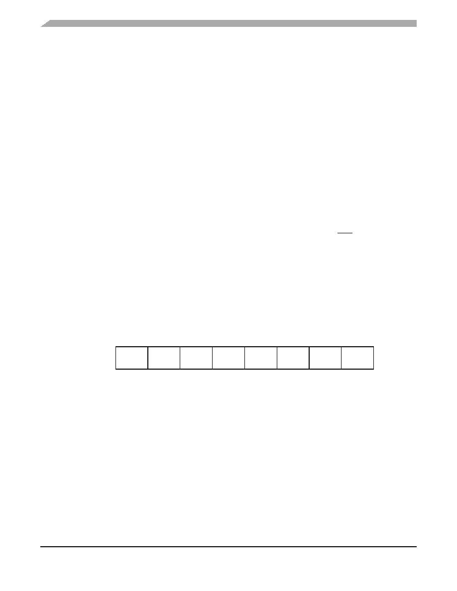
2.11 FLASH Block Protect Register
The FLASH block protect register (FLBPR) is implemented as a byte within the FLASH memory, and
therefore can be written only during a programming sequence of the FLASH memory. The value in this
register determines the starting location of the protected range within the FLASH memory.
BPR7–BPR0 — FLASH Block Protect Bits
These eight bits represent bits 13–6 of a 16-bit memory address. Bits 15 and 14 are 1s and bits 5–0
are 0s.
The resultant 16-bit address is used for specifying the start address of the FLASH memory for block
protection. The FLASH is protected from this start address to the end of FLASH memory, at $FFFF.
With this mechanism, the protect start address can be $XX00, $XX40, etc., (64 bytes page boundaries)
within the FLASH memory. See Figure 2-6 and Table 2-2.
Address:
$FF7E
Bit 7
654321
Bit 0
Read:
BPR7
BPR6
BPR5
BPR4
BPR3
BPR2
BPR1
BPR0
Write:
Reset:
UUUUUUUU
U = Unaffected by reset. Initial value from factory is 1.
Write to this register is by a programming sequence to the FLASH memory.
Figure 2-5. FLASH Block Protect Register (FLBPR)
相关PDF资料 |
PDF描述 |
|---|---|
| MC9S08AW48CFDE | IC MCU 48K FLASH 48-QFN |
| MC908JK1EMDWE | IC MCU 1.5K FLASH 8MHZ 20-SOIC |
| HC55142IMZ96 | IC SLIC UNIVERSAL LP 28-PLCC |
| HC55142IMZ | IC SLIC UNIVERSAL LP 28-PLCC |
| S9S08AW32E5MPUE | MCU 32K FLASH AUTO MONET 64-LQFP |
相关代理商/技术参数 |
参数描述 |
|---|---|
| MC908KX2CPE | 功能描述:IC MCU 2K FLASH 8MHZ SCI 16-DIP RoHS:是 类别:集成电路 (IC) >> 嵌入式 - 微控制器, 系列:HC08 标准包装:1 系列:87C 核心处理器:MCS 51 芯体尺寸:8-位 速度:16MHz 连通性:SIO 外围设备:- 输入/输出数:32 程序存储器容量:8KB(8K x 8) 程序存储器类型:OTP EEPROM 大小:- RAM 容量:256 x 8 电压 - 电源 (Vcc/Vdd):4 V ~ 6 V 数据转换器:- 振荡器型:外部 工作温度:0°C ~ 70°C 封装/外壳:44-DIP 包装:管件 其它名称:864285 |
| MC908KX2MDWE | 功能描述:8位微控制器 -MCU 8BIT MCU W/2K FLASH EPP RoHS:否 制造商:Silicon Labs 核心:8051 处理器系列:C8051F39x 数据总线宽度:8 bit 最大时钟频率:50 MHz 程序存储器大小:16 KB 数据 RAM 大小:1 KB 片上 ADC:Yes 工作电源电压:1.8 V to 3.6 V 工作温度范围:- 40 C to + 105 C 封装 / 箱体:QFN-20 安装风格:SMD/SMT |
| MC908KX2MDWER | 功能描述:8位微控制器 -MCU 8BIT MCU W/2K FLASH EPP RoHS:否 制造商:Silicon Labs 核心:8051 处理器系列:C8051F39x 数据总线宽度:8 bit 最大时钟频率:50 MHz 程序存储器大小:16 KB 数据 RAM 大小:1 KB 片上 ADC:Yes 工作电源电压:1.8 V to 3.6 V 工作温度范围:- 40 C to + 105 C 封装 / 箱体:QFN-20 安装风格:SMD/SMT |
| MC908KX2VDWE | 功能描述:8位微控制器 -MCU 8BIT MCU W/2K FLASH EPP RoHS:否 制造商:Silicon Labs 核心:8051 处理器系列:C8051F39x 数据总线宽度:8 bit 最大时钟频率:50 MHz 程序存储器大小:16 KB 数据 RAM 大小:1 KB 片上 ADC:Yes 工作电源电压:1.8 V to 3.6 V 工作温度范围:- 40 C to + 105 C 封装 / 箱体:QFN-20 安装风格:SMD/SMT |
| MC908KX2VDWER | 制造商:Freescale Semiconductor 功能描述:8-BIT HC08 CISC 2KB FLASH 3.3V/5V 16-PIN SOIC W T/R - Tape and Reel |
发布紧急采购,3分钟左右您将得到回复。