- 您现在的位置:买卖IC网 > PDF目录10990 > MC908QB4MDWE (Freescale Semiconductor)IC MCU 8BIT 4K FLASH 16-SOIC PDF资料下载
参数资料
| 型号: | MC908QB4MDWE |
| 厂商: | Freescale Semiconductor |
| 文件页数: | 71/232页 |
| 文件大小: | 0K |
| 描述: | IC MCU 8BIT 4K FLASH 16-SOIC |
| 标准包装: | 47 |
| 系列: | HC08 |
| 核心处理器: | HC08 |
| 芯体尺寸: | 8-位 |
| 速度: | 8MHz |
| 连通性: | SCI,SPI |
| 外围设备: | LVD,POR,PWM |
| 输入/输出数: | 13 |
| 程序存储器容量: | 4KB(4K x 8) |
| 程序存储器类型: | 闪存 |
| RAM 容量: | 128 x 8 |
| 电压 - 电源 (Vcc/Vdd): | 2.7 V ~ 5.5 V |
| 数据转换器: | A/D 10x10b |
| 振荡器型: | 内部 |
| 工作温度: | -40°C ~ 125°C |
| 封装/外壳: | 16-SOIC(0.295",7.50mm 宽) |
| 包装: | 管件 |
第1页第2页第3页第4页第5页第6页第7页第8页第9页第10页第11页第12页第13页第14页第15页第16页第17页第18页第19页第20页第21页第22页第23页第24页第25页第26页第27页第28页第29页第30页第31页第32页第33页第34页第35页第36页第37页第38页第39页第40页第41页第42页第43页第44页第45页第46页第47页第48页第49页第50页第51页第52页第53页第54页第55页第56页第57页第58页第59页第60页第61页第62页第63页第64页第65页第66页第67页第68页第69页第70页当前第71页第72页第73页第74页第75页第76页第77页第78页第79页第80页第81页第82页第83页第84页第85页第86页第87页第88页第89页第90页第91页第92页第93页第94页第95页第96页第97页第98页第99页第100页第101页第102页第103页第104页第105页第106页第107页第108页第109页第110页第111页第112页第113页第114页第115页第116页第117页第118页第119页第120页第121页第122页第123页第124页第125页第126页第127页第128页第129页第130页第131页第132页第133页第134页第135页第136页第137页第138页第139页第140页第141页第142页第143页第144页第145页第146页第147页第148页第149页第150页第151页第152页第153页第154页第155页第156页第157页第158页第159页第160页第161页第162页第163页第164页第165页第166页第167页第168页第169页第170页第171页第172页第173页第174页第175页第176页第177页第178页第179页第180页第181页第182页第183页第184页第185页第186页第187页第188页第189页第190页第191页第192页第193页第194页第195页第196页第197页第198页第199页第200页第201页第202页第203页第204页第205页第206页第207页第208页第209页第210页第211页第212页第213页第214页第215页第216页第217页第218页第219页第220页第221页第222页第223页第224页第225页第226页第227页第228页第229页第230页第231页第232页
Serial Peripheral Interface (SPI) Module
MC68HC908QB8 Data Sheet, Rev. 3
160
Freescale Semiconductor
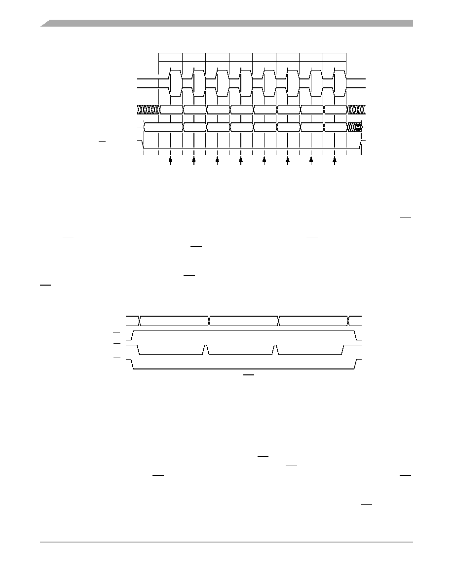
Figure 15-4. Transmission Format (CPHA = 0)
Two waveforms are shown for SPSCK: one for CPOL = 0 and another for CPOL = 1. The diagram may
be interpreted as a master or slave timing diagram because the serial clock (SPSCK), master in/slave out
(MISO), and master out/slave in (MOSI) pins are directly connected between the master and the slave.
The MISO signal is the output from the slave, and the MOSI signal is the output from the master. The SS
line is the slave select input to the slave. The slave SPI drives its MISO output only when its slave select
input (SS) is low, so that only the selected slave drives to the master. The SS pin of the master is not
shown but is assumed to be inactive. The SS pin of the master must be high or must be reconfigured as
general-purpose I/O not affecting the SPI. (See 15.3.6.2 Mode Fault Error.) When CPHA = 0, the first
SPSCK edge is the MSB capture strobe. Therefore, the slave must begin driving its data before the first
SPSCK edge, and a falling edge on the SS pin is used to start the slave data transmission. The slave’s
SS pin must be toggled back to high and then low again between each byte transmitted as shown in
Figure 15-5. CPHA/SS Timing
15.3.3.3 Transmission Format When CPHA = 1
Figure 15-6 shows an SPI transmission in which CPHA = 1. The figure should not be used as a
replacement for data sheet parametric information. Two waveforms are shown for SPSCK: one for
CPOL = 0 and another for CPOL = 1. The diagram may be interpreted as a master or slave timing
diagram because the serial clock (SPSCK), master in/slave out (MISO), and master out/slave in (MOSI)
pins are directly connected between the master and the slave. The MISO signal is the output from the
slave, and the MOSI signal is the output from the master. The SS line is the slave select input to the slave.
The slave SPI drives its MISO output only when its slave select input (SS) is low, so that only the selected
slave drives to the master. The SS pin of the master is not shown but is assumed to be inactive. The SS
pin of the master must be high or must be reconfigured as general-purpose I/O not affecting the SPI. (See
15.3.6.2 Mode Fault Error.) When CPHA = 1, the master begins driving its MOSI pin on the first SPSCK
edge. Therefore, the slave uses the first SPSCK edge as a start transmission signal. The SS pin can
BIT 6
BIT 5
BIT 4
BIT 3
BIT 2
BIT 1
LSB
MSB
BIT 6
BIT 5
BIT 4
BIT 3
BIT 2
BIT 1
LSB
MSB
123
4
5
6
7
8
SPSCK CYCLE #
FOR REFERENCE
SPSCK; CPOL = 0
SPSCK; CPOL =1
MOSI
FROM MASTER
MISO
FROM SLAVE
SS; TO SLAVE
CAPTURE STROBE
BYTE 1
BYTE 3
MISO/MOSI
BYTE 2
MASTER SS
SLAVE SS
CPHA = 0
SLAVE SS
CPHA = 1
相关PDF资料 |
PDF描述 |
|---|---|
| MC9S08AW48CFUER | IC MCU 48K FLASH 64-QFP |
| MC9S08JE128VLK | IC MCU 8BIT 128K FLASH 80LQFP |
| MCF51QE96CLK | IC MCU 32BIT 96K FLASH 80-LQFP |
| VI-B4H-IY-F3 | CONVERTER MOD DC/DC 52V 50W |
| VI-B4H-IY-F1 | CONVERTER MOD DC/DC 52V 50W |
相关代理商/技术参数 |
参数描述 |
|---|---|
| MC908QB8 | 制造商:FREESCALE 制造商全称:Freescale Semiconductor, Inc 功能描述:To provide the most up-to-date information, the revision of our documents |
| MC908QB8CDT | 制造商:Freescale Semiconductor 功能描述:8-BIT HC08 CISC 8KB FLASH 16-PIN TSSOP RAIL - Trays |
| MC908QB8CDTE | 功能描述:8位微控制器 -MCU NITRON 8K FLASH 908QB8 RoHS:否 制造商:Silicon Labs 核心:8051 处理器系列:C8051F39x 数据总线宽度:8 bit 最大时钟频率:50 MHz 程序存储器大小:16 KB 数据 RAM 大小:1 KB 片上 ADC:Yes 工作电源电压:1.8 V to 3.6 V 工作温度范围:- 40 C to + 105 C 封装 / 箱体:QFN-20 安装风格:SMD/SMT |
| MC908QB8CDWE | 功能描述:8位微控制器 -MCU NITRON 8K FLASH 908QB8 RoHS:否 制造商:Silicon Labs 核心:8051 处理器系列:C8051F39x 数据总线宽度:8 bit 最大时钟频率:50 MHz 程序存储器大小:16 KB 数据 RAM 大小:1 KB 片上 ADC:Yes 工作电源电压:1.8 V to 3.6 V 工作温度范围:- 40 C to + 105 C 封装 / 箱体:QFN-20 安装风格:SMD/SMT |
| MC908QB8CDWER | 功能描述:8位微控制器 -MCU NITRN 8K FLSH 908QB8 RoHS:否 制造商:Silicon Labs 核心:8051 处理器系列:C8051F39x 数据总线宽度:8 bit 最大时钟频率:50 MHz 程序存储器大小:16 KB 数据 RAM 大小:1 KB 片上 ADC:Yes 工作电源电压:1.8 V to 3.6 V 工作温度范围:- 40 C to + 105 C 封装 / 箱体:QFN-20 安装风格:SMD/SMT |
发布紧急采购,3分钟左右您将得到回复。