- 您现在的位置:买卖IC网 > PDF目录11934 > MC908QY4AMDTER (Freescale Semiconductor)IC MCU 8BIT CISC 8-SOEIAJ PDF资料下载
参数资料
| 型号: | MC908QY4AMDTER |
| 厂商: | Freescale Semiconductor |
| 文件页数: | 150/202页 |
| 文件大小: | 0K |
| 描述: | IC MCU 8BIT CISC 8-SOEIAJ |
| 标准包装: | 2,500 |
| 系列: | HC08 |
| 核心处理器: | HC08 |
| 芯体尺寸: | 8-位 |
| 速度: | 8MHz |
| 外围设备: | LVD,POR,PWM |
| 输入/输出数: | 13 |
| 程序存储器容量: | 4KB(4K x 8) |
| 程序存储器类型: | 闪存 |
| RAM 容量: | 128 x 8 |
| 电压 - 电源 (Vcc/Vdd): | 2.7 V ~ 5.5 V |
| 数据转换器: | A/D 6x10b |
| 振荡器型: | 内部 |
| 工作温度: | -40°C ~ 125°C |
| 封装/外壳: | 16-TSSOP(0.173",4.40mm 宽) |
| 包装: | 带卷 (TR) |
第1页第2页第3页第4页第5页第6页第7页第8页第9页第10页第11页第12页第13页第14页第15页第16页第17页第18页第19页第20页第21页第22页第23页第24页第25页第26页第27页第28页第29页第30页第31页第32页第33页第34页第35页第36页第37页第38页第39页第40页第41页第42页第43页第44页第45页第46页第47页第48页第49页第50页第51页第52页第53页第54页第55页第56页第57页第58页第59页第60页第61页第62页第63页第64页第65页第66页第67页第68页第69页第70页第71页第72页第73页第74页第75页第76页第77页第78页第79页第80页第81页第82页第83页第84页第85页第86页第87页第88页第89页第90页第91页第92页第93页第94页第95页第96页第97页第98页第99页第100页第101页第102页第103页第104页第105页第106页第107页第108页第109页第110页第111页第112页第113页第114页第115页第116页第117页第118页第119页第120页第121页第122页第123页第124页第125页第126页第127页第128页第129页第130页第131页第132页第133页第134页第135页第136页第137页第138页第139页第140页第141页第142页第143页第144页第145页第146页第147页第148页第149页当前第150页第151页第152页第153页第154页第155页第156页第157页第158页第159页第160页第161页第162页第163页第164页第165页第166页第167页第168页第169页第170页第171页第172页第173页第174页第175页第176页第177页第178页第179页第180页第181页第182页第183页第184页第185页第186页第187页第188页第189页第190页第191页第192页第193页第194页第195页第196页第197页第198页第199页第200页第201页第202页
Registers
MC68HC908QYA/QTA Family Data Sheet, Rev. 3
Freescale Semiconductor
49
ADIV[1:0] — ADC10 Clock Divider Bits
ADIV1 and ADIV0 select the divide ratio used by the ADC10 to generate the internal clock ADCK.
Table 3-3 shows the available clock configurations.
ADICLK — Input Clock Select Bit
If ACLKEN is clear, ADICLK selects either the bus clock or an alternate clock source as the input clock
source to generate the internal clock ADCK. If the alternate clock source is less than the minimum
clock speed, use the internally-generated bus clock as the clock source. As long as the internal clock
ADCK, which is equal to the selected input clock divided by ADIV, is at a frequency (fADCK) between
the minimum and maximum clock speeds (considering ALPC), correct operation can be guaranteed.
1 = The internal bus clock is selected as the input clock source
0 = The alternate clock source IS SELECTED
MODE[1:0] — 10- or 8-Bit or Hardware Triggered Mode Selection
These bits select 10- or 8-bit operation. The successive approximation converter generates a result
that is rounded to 8- or 10-bit value based on the mode selection. This rounding process sets the
transfer function to transition at the midpoint between the ideal code voltages, causing a quantization
error of ± 1/2LSB.
Reset returns 8-bit mode.
00 = 8-bit, right-justified, ADSCR software triggered mode enabled
01 = 10-bit, right-justified, ADSCR software triggered mode enabled
10 = Reserved
11 = 10-bit, right-justified, hardware triggered mode enabled
ADLSMP — Long Sample Time Configuration
This bit configures the sample time of the ADC10 to either 3.5 or 23.5 ADCK clock cycles. This adjusts
the sample period to allow higher impedance inputs to be accurately sampled or to maximize
conversion speed for lower impedance inputs. Longer sample times can also be used to lower overall
power consumption in continuous conversion mode if high conversion rates are not required.
1 = Long sample time (23.5 cycles)
0 = Short sample time (3.5 cycles)
ACLKEN — Asynchronous Clock Source Enable
This bit enables the asynchronous clock source as the input clock to generate the internal clock ADCK,
and allows operation in stop mode. The asynchronous clock source will operate between 1 MHz and
2 MHz if ADLPC is clear, and between 0.5 MHz and 1 MHz if ADLPC is set.
1 = The asynchronous clock is selected as the input clock source (the clock generator is only
enabled during the conversion)
0 = ADICLK specifies the input clock source and conversions will not continue in stop mode
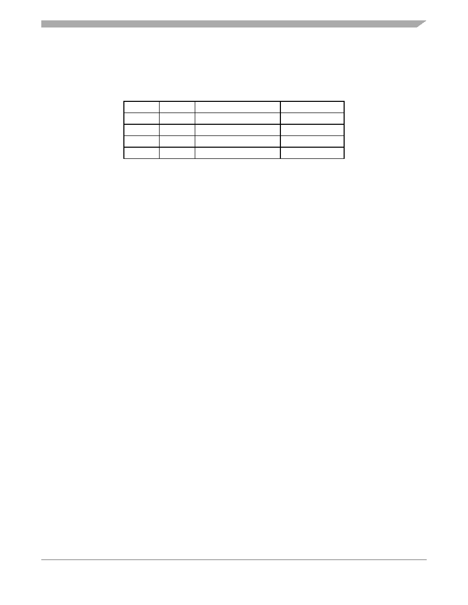
Table 3-3. ADC10 Clock Divide Ratio
ADIV1
ADIV0
Divide Ratio (ADIV)
Clock Rate
0
1
Input clock
÷ 1
0
1
2
Input clock
÷ 2
1
0
4
Input clock
÷ 4
1
8
Input clock
÷ 8
相关PDF资料 |
PDF描述 |
|---|---|
| MC9S08GT16AMFCE | IC MCU 16K FLASH 2K RAM 32-QFN |
| V72A24T400B2 | CONVERTER MOD DC/DC 24V 400W |
| MC908QT2AMDWER | IC MCU 8BIT 1.5K FLASH 8-SOIC |
| V72A24T400B | CONVERTER MOD DC/DC 24V 400W |
| V72A36T400BG3 | CONVERTER MOD DC/DC 36V 400W |
相关代理商/技术参数 |
参数描述 |
|---|---|
| MC908QY4AMDWE | 功能描述:8位微控制器 -MCU CI 908QY4A SOG RoHS:否 制造商:Silicon Labs 核心:8051 处理器系列:C8051F39x 数据总线宽度:8 bit 最大时钟频率:50 MHz 程序存储器大小:16 KB 数据 RAM 大小:1 KB 片上 ADC:Yes 工作电源电压:1.8 V to 3.6 V 工作温度范围:- 40 C to + 105 C 封装 / 箱体:QFN-20 安装风格:SMD/SMT |
| MC908QY4AMDWER | 功能描述:8位微控制器 -MCU CI 908QY4A SOG RoHS:否 制造商:Silicon Labs 核心:8051 处理器系列:C8051F39x 数据总线宽度:8 bit 最大时钟频率:50 MHz 程序存储器大小:16 KB 数据 RAM 大小:1 KB 片上 ADC:Yes 工作电源电压:1.8 V to 3.6 V 工作温度范围:- 40 C to + 105 C 封装 / 箱体:QFN-20 安装风格:SMD/SMT |
| MC908QY4AMFQE | 制造商:FREESCALE 制造商全称:Freescale Semiconductor, Inc 功能描述:M68HC08 Microcontrollers |
| MC908QY4AMPE | 功能描述:8位微控制器 -MCU NITRON CI 908QY4A SOG RoHS:否 制造商:Silicon Labs 核心:8051 处理器系列:C8051F39x 数据总线宽度:8 bit 最大时钟频率:50 MHz 程序存储器大小:16 KB 数据 RAM 大小:1 KB 片上 ADC:Yes 工作电源电压:1.8 V to 3.6 V 工作温度范围:- 40 C to + 105 C 封装 / 箱体:QFN-20 安装风格:SMD/SMT |
| MC908QY4CDTE | 制造商:FREESCALE 制造商全称:Freescale Semiconductor, Inc 功能描述:M68HC08 Microcontrollers |
发布紧急采购,3分钟左右您将得到回复。