- 您现在的位置:买卖IC网 > PDF目录45285 > MC9328MXLDVP20R2 (FREESCALE SEMICONDUCTOR INC) 32-BIT, 200 MHz, RISC PROCESSOR, PBGA225 PDF资料下载
参数资料
| 型号: | MC9328MXLDVP20R2 |
| 厂商: | FREESCALE SEMICONDUCTOR INC |
| 元件分类: | 微控制器/微处理器 |
| 英文描述: | 32-BIT, 200 MHz, RISC PROCESSOR, PBGA225 |
| 封装: | 13 X 13 MM, 0.80 MM PITCH, ROHS COMPLIANT, PLASTIC, MAPBGA-225 |
| 文件页数: | 9/90页 |
| 文件大小: | 1242K |
| 代理商: | MC9328MXLDVP20R2 |
第1页第2页第3页第4页第5页第6页第7页第8页当前第9页第10页第11页第12页第13页第14页第15页第16页第17页第18页第19页第20页第21页第22页第23页第24页第25页第26页第27页第28页第29页第30页第31页第32页第33页第34页第35页第36页第37页第38页第39页第40页第41页第42页第43页第44页第45页第46页第47页第48页第49页第50页第51页第52页第53页第54页第55页第56页第57页第58页第59页第60页第61页第62页第63页第64页第65页第66页第67页第68页第69页第70页第71页第72页第73页第74页第75页第76页第77页第78页第79页第80页第81页第82页第83页第84页第85页第86页第87页第88页第89页第90页
Electrical Characteristics
MC9328MXL Technical Data, Rev. 8
Freescale Semiconductor
17
3
Electrical Characteristics
This section contains the electrical specifications and timing diagrams for the i.MXL processor.
3.1
Maximum Ratings
Table 4 provides information on maximum ratings which are those values beyond which damage to the
device may occur. Functional operation should be restricted to the limits listed in Recommended Operating
Range Table 5 on page 18 or the DC Characteristics table.
3.2
Recommended Operating Range
Table 5 provides the recommended operating ranges for the supply voltages and temperatures. The i.MXL
processor has multiple pairs of VDD and VSS power supply and return pins. QVDD and QVSS pins are
used for internal logic. All other VDD and VSS pins are for the I/O pads voltage supply, and each pair of
VDD and VSS provides power to the enclosed I/O pads. This design allows different peripheral supply
voltage levels in a system.
Because AVDD pins are supply voltages to the analog pads, it is recommended to isolate and noise-filter
the AVDD pins from other VDD pins.
For more information about I/O pads grouping per VDD, please refer to Table 2 on page 4.
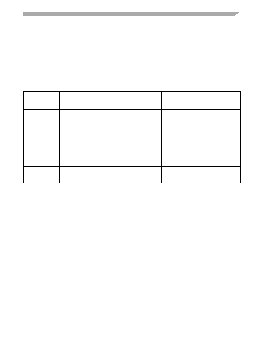
Table 4. Maximum Ratings
Symbol
Rating
Minimum
Maximum
Unit
NVDD
DC I/O Supply Voltage
-0.3
3.3
V
QVDD
DC Internal (core = 150 MHz) Supply Voltage
-0.3
1.9
V
QVDD
DC Internal (core = 200 MHz) Supply Voltage
-0.3
2.0
V
AVDD
DC Analog Supply Voltage
-0.3
3.3
V
BTRFVDD
DC Bluetooth Supply Voltage
-0.3
3.3
V
VESD_HBM
ESD immunity with HBM (human body model)
–
2000
V
VESD_MM
ESD immunity with MM (machine model)
–
100
V
ILatchup
Latch-up immunity
–
200
mA
Test
Storage temperature
-55
150
°C
Pmax
Power Consumption
8001
1 A typical application with 30 pads simultaneously switching assumes the GPIO toggling and instruction fetches from the ARM
core-that is, 7x GPIO, 15x Data bus, and 8x Address bus.
13002
2 A worst-case application with 70 pads simultaneously switching assumes the GPIO toggling and instruction fetches from the
ARM core-that is, 32x GPIO, 30x Data bus, 8x Address bus. These calculations are based on the core running its heaviest OS
application at 200MHz, and where the whole image is running out of SDRAM. QVDD at 2.0V, NVDD and AVDD at 3.3V,
therefore, 180mA is the worst measurement recorded in the factory environment, max 5mA is consumed for OSC pads, with
each toggle GPIO consuming 4mA.
mW
Because
of
an
order
from
the
United
States
International
Trade
Commission,
BGA-packaged
product
lines
and
part
numbers
indicated
here
currently
are
not
available
from
Freescale
for
import
or
sale
in
the
United
States
prior
to
September
2010:
i.MXL
Product
Family
相关PDF资料 |
PDF描述 |
|---|---|
| MC9328MXLDVM20R2 | 32-BIT, 200 MHz, RISC PROCESSOR, PBGA256 |
| MC9328MXLDVM15 | 150 MHz, RISC PROCESSOR, PBGA256 |
| MC9328MXLVH15 | 32-BIT, 150 MHz, RISC PROCESSOR, PBGA256 |
| MC9328MXLDVP15 | 150 MHz, RISC PROCESSOR, PBGA225 |
| MC9328MXLDVF15 | 150 MHz, RISC PROCESSOR, PBGA225 |
相关代理商/技术参数 |
参数描述 |
|---|---|
| MC9328MXLP/D | 制造商:FREESCALE 制造商全称:Freescale Semiconductor, Inc 功能描述:i.MX Integrated Portable System Processor |
| MC9328MXLRM/D | 制造商:FREESCALE 制造商全称:Freescale Semiconductor, Inc 功能描述:i.MX Integrated Portable System Processor |
| MC9328MXLVF20 | 制造商:Rochester Electronics LLC 功能描述:DRAGONBALL CORSICA 225 - Bulk 制造商:Motorola Inc 功能描述: |
| MC9328MXLVF20R2 | 制造商:Rochester Electronics LLC 功能描述:DRAGONBALL CORSICA 225 - Bulk |
| MC9328MXLVH15 | 制造商:FREESCALE-SEMI 功能描述: |
发布紧急采购,3分钟左右您将得到回复。