- 您现在的位置:买卖IC网 > PDF目录10951 > MC9328MXLVM15R2 (Freescale Semiconductor)IC MCU I.MX 150MHZ 256-MAPBGA PDF资料下载
参数资料
| 型号: | MC9328MXLVM15R2 |
| 厂商: | Freescale Semiconductor |
| 文件页数: | 79/90页 |
| 文件大小: | 0K |
| 描述: | IC MCU I.MX 150MHZ 256-MAPBGA |
| 标准包装: | 1,000 |
| 系列: | i.MXL |
| 核心处理器: | ARM9 |
| 芯体尺寸: | 32-位 |
| 速度: | 150MHz |
| 连通性: | EBI/EMI,I²C,MMC/SD,SPI,SSI,UART/USART,USB |
| 外围设备: | DMA,I²S,LCD,POR,PWM,WDT |
| 输入/输出数: | 97 |
| 程序存储器类型: | ROMless |
| 电压 - 电源 (Vcc/Vdd): | 1.7 V ~ 3.3 V |
| 振荡器型: | 外部 |
| 工作温度: | 0°C ~ 70°C |
| 封装/外壳: | 225-LFBGA |
| 包装: | 带卷 (TR) |
第1页第2页第3页第4页第5页第6页第7页第8页第9页第10页第11页第12页第13页第14页第15页第16页第17页第18页第19页第20页第21页第22页第23页第24页第25页第26页第27页第28页第29页第30页第31页第32页第33页第34页第35页第36页第37页第38页第39页第40页第41页第42页第43页第44页第45页第46页第47页第48页第49页第50页第51页第52页第53页第54页第55页第56页第57页第58页第59页第60页第61页第62页第63页第64页第65页第66页第67页第68页第69页第70页第71页第72页第73页第74页第75页第76页第77页第78页当前第79页第80页第81页第82页第83页第84页第85页第86页第87页第88页第89页第90页
Functional Description and Application Information
MC9328MXL Technical Data, Rev. 8
80
Freescale Semiconductor
4.14
CMOS Sensor Interface
The CMOS Sensor Interface (CSI) module consists of a control register to configure the interface timing,
a control register for statistic data generation, a status register, interface logic, a 32
× 32 image data receive
FIFO, and a 16
× 32 statistic data FIFO.
4.14.1
Gated Clock Mode
Figure 63 shows the timing diagram when the CMOS sensor output data is configured for negative edge
and the CSI is programmed to received data on the positive edge. Figure 64 shows the timing diagram
when the CMOS sensor output data is configured for positive edge and the CSI is programmed to received
data in negative edge. The parameters for the timing diagrams are listed in Table 35.
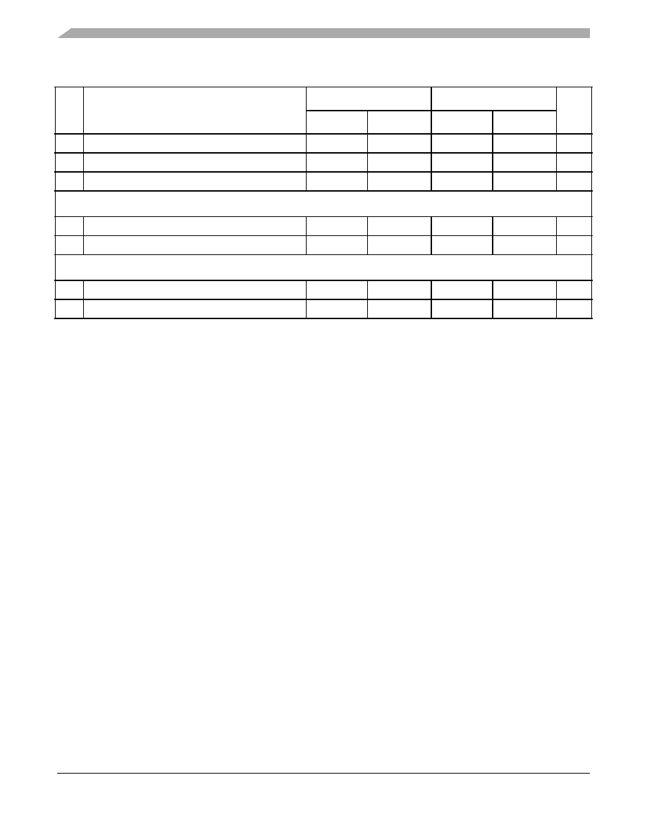
28
STCK high to STXD high impedance
17.90
29.75
15.7
26.1
ns
29
SRXD setup time before SRCK low
1.14
–
1.0
–
ns
30
SRXD hold time after SRCK low
0
–
0
–
ns
Synchronous Internal Clock Operation (Port B Alternate Function2)
31
SRXD setup before STCK falling
18.81
–
16.5
–
ns
32
SRXD hold after STCK falling
0
–
0
–
ns
Synchronous External Clock Operation (Port B Alternate Function2)
33
SRXD setup before STCK falling
1.14
–
1.0
–
ns
34
SRXD hold after STCK falling
0
–
0
–
ns
1 All the timings for the SSI are given for a non-inverted serial clock polarity (TSCKP/RSCKP = 0) and a non-inverted frame sync
(TFSI/RFSI = 0). If the polarity of the clock and/or the frame sync have been inverted, all the timing remains valid by inverting
the clock signal STCK/SRCK and/or the frame sync STFS/SRFS shown in the tables and in the figures.
2 There are 2 set of I/O signals for the SSI module. They are from Port C primary function (pad 257 to pad 261) and Port B
alternate function (pad 283 to pad 288). When SSI signals are configured as outputs, they can be viewed both at Port C primary
function and Port B alternate function. When SSI signals are configured as inputs, the SSI module selects the input based on
FMCR register bits in the Clock controller module (CRM). By default, the input are selected from Port C primary function.
3
bl = bit length; wl = word length.
Table 34. SSI (Port B Alternate Function) Timing Parameter Table (Continued)
Ref
No.
Parameter
1.8 ± 0.1 V
3.0 ± 0.3 V
Unit
Minimum
Maximum
Minimum
Maximum
相关PDF资料 |
PDF描述 |
|---|---|
| VI-26D-IY-F2 | CONVERTER MOD DC/DC 85V 50W |
| VI-26B-IY-F2 | CONVERTER MOD DC/DC 95V 50W |
| MC9328MXLDVM15R2 | IC MCU I.MX 150MHZ 256-MAPBGA |
| VI-264-IY-F1 | CONVERTER MOD DC/DC 48V 50W |
| VI-B52-IX-B1 | CONVERTER MOD DC/DC 15V 75W |
相关代理商/技术参数 |
参数描述 |
|---|---|
| MC9328MXLVM20 | 功能描述:处理器 - 专门应用 DRAGONBALL CORSICA PB-FR RoHS:否 制造商:Freescale Semiconductor 类型:Multimedia Applications 核心:ARM Cortex A9 处理器系列:i.MX6 数据总线宽度:32 bit 最大时钟频率:1 GHz 指令/数据缓存: 数据 RAM 大小:128 KB 数据 ROM 大小: 工作电源电压: 最大工作温度:+ 95 C 安装风格:SMD/SMT 封装 / 箱体:MAPBGA-432 |
| MC9328MXLVM20 | 制造商:Freescale Semiconductor 功能描述:Microprocessor |
| MC9328MXLVM20R2 | 功能描述:处理器 - 专门应用 DRAGONBALL CORSICA PB-FR RoHS:否 制造商:Freescale Semiconductor 类型:Multimedia Applications 核心:ARM Cortex A9 处理器系列:i.MX6 数据总线宽度:32 bit 最大时钟频率:1 GHz 指令/数据缓存: 数据 RAM 大小:128 KB 数据 ROM 大小: 工作电源电压: 最大工作温度:+ 95 C 安装风格:SMD/SMT 封装 / 箱体:MAPBGA-432 |
| MC9328MXLVP15 | 功能描述:处理器 - 专门应用 DRAGONBALL MXL 225 PB-FR RoHS:否 制造商:Freescale Semiconductor 类型:Multimedia Applications 核心:ARM Cortex A9 处理器系列:i.MX6 数据总线宽度:32 bit 最大时钟频率:1 GHz 指令/数据缓存: 数据 RAM 大小:128 KB 数据 ROM 大小: 工作电源电压: 最大工作温度:+ 95 C 安装风格:SMD/SMT 封装 / 箱体:MAPBGA-432 |
| MC9328MXLVP15 | 制造商:Freescale Semiconductor 功能描述:Microprocessor |
发布紧急采购,3分钟左右您将得到回复。