- 您现在的位置:买卖IC网 > PDF目录3791 > MC9S08AC96CFGE (Freescale Semiconductor)MCU 96K FLASH 8K RAM 44-LQFP PDF资料下载
参数资料
| 型号: | MC9S08AC96CFGE |
| 厂商: | Freescale Semiconductor |
| 文件页数: | 6/40页 |
| 文件大小: | 0K |
| 描述: | MCU 96K FLASH 8K RAM 44-LQFP |
| 标准包装: | 160 |
| 系列: | S08 |
| 核心处理器: | S08 |
| 芯体尺寸: | 8-位 |
| 速度: | 40MHz |
| 连通性: | I²C,LIN,SCI,SPI |
| 外围设备: | LVD,POR,PWM,WDT |
| 输入/输出数: | 38 |
| 程序存储器容量: | 96KB(96K x 8) |
| 程序存储器类型: | 闪存 |
| RAM 容量: | 6K x 8 |
| 电压 - 电源 (Vcc/Vdd): | 2.7 V ~ 5.5 V |
| 数据转换器: | A/D 8x10b |
| 振荡器型: | 内部 |
| 工作温度: | -40°C ~ 85°C |
| 封装/外壳: | 44-LQFP |
| 包装: | 托盘 |
第1页第2页第3页第4页第5页当前第6页第7页第8页第9页第10页第11页第12页第13页第14页第15页第16页第17页第18页第19页第20页第21页第22页第23页第24页第25页第26页第27页第28页第29页第30页第31页第32页第33页第34页第35页第36页第37页第38页第39页第40页
Chapter 3 Electrical Characteristics and Timing Specifications
MC9S08AC128 Series Data Sheet, Rev. 4
14
Freescale Semiconductor
Solving equations 1 and 2 for K gives:
K = PD (TA + 273C) + JA (PD)
2
Eqn. 3-3
where K is a constant pertaining to the particular part. K can be determined from equation 3 by measuring PD (at equilibrium)
for a known TA. Using this value of K, the values of PD and TJ can be obtained by solving equations 1 and 2 iteratively for any
value of TA.
3.5
ESD Protection and Latch-Up Immunity
Although damage from electrostatic discharge (ESD) is much less common on these devices than on early CMOS circuits,
normal handling precautions should be used to avoid exposure to static discharge. Qualification tests are performed to ensure
that these devices can withstand exposure to reasonable levels of static without suffering any permanent damage.
All ESD testing is in conformity with AEC-Q100 Stress Test Qualification for Automotive Grade Integrated Circuits and
JEDEC Standard for Non-Automotive Grade Integrated Circuits. During the device qualification ESD stresses were performed
for the Human Body Model (HBM), the Machine Model (MM) and the Charge Device Model (CDM).
A device is defined as a failure if after exposure to ESD pulses the device no longer meets the device specification. Complete
DC parametric and functional testing is performed per the applicable device specification at room temperature followed by hot
temperature, unless specified otherwise in the device specification.
3.6
DC Characteristics
This section includes information about power supply requirements, I/O pin characteristics, and power supply current in various
operating modes.
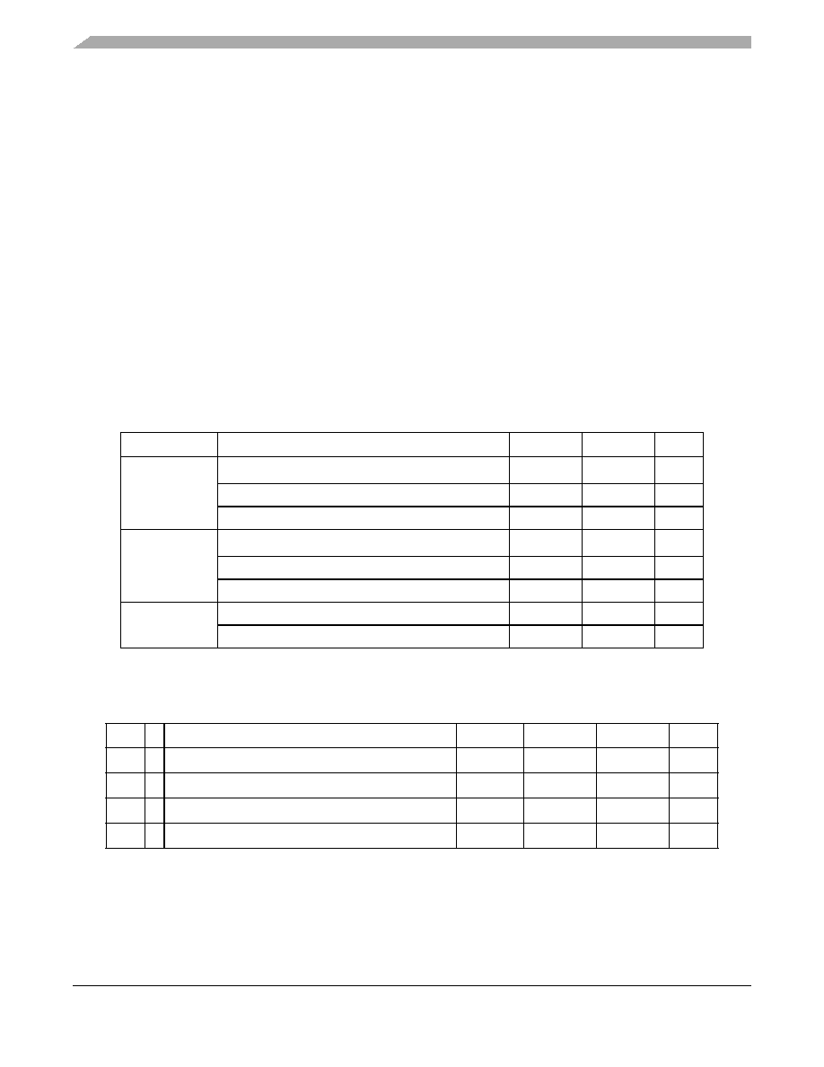
Table 3-4. ESD and Latch-up Test Conditions
Model
Description
Symbol
Value
Unit
Human Body
Series Resistance
R1
1500
Storage Capacitance
C
100
pF
Number of Pulse per pin
–
3
Machine
Series Resistance
R1
0
Storage Capacitance
C
200
pF
Number of Pulse per pin
–
3
Latch-up
Minimum input voltage limit
– 2.5
V
Maximum input voltage limit
7.5
V
Table 3-5. ESD and Latch-Up Protection Characteristics
Num C
Rating
Symbol
Min
Max
Unit
1
C Human Body Model (HBM)
VHBM
2000
–
V
2
C Machine Model (MM)
VMM
200
–
V
3
C Charge Device Model (CDM)
VCDM
500
–
V
4C Latch-up Current at TA = 125CILAT
100
–
mA
相关PDF资料 |
PDF描述 |
|---|---|
| MC9S08QE96CLD | IC MCU 8BIT 96K FLASH 44-LQFP |
| MC9S08DV16ACLCR | MCU 8BIT 16K FLASH 32-LQFP |
| MC908JL16CDWE | IC MCU 16K FLASH 8MHZ 28-SOIC |
| MC9S08DV128MLL | MCU 8BIT 128K FLASH 100-LQFP |
| MC9S08DV128MLF | MCU 8BIT 128K FLASH 48-LQFP |
相关代理商/技术参数 |
参数描述 |
|---|---|
| MC9S08AC96CFGER | 制造商:Freescale Semiconductor 功能描述:96K FLASH, 8K RAM - Tape and Reel |
| MC9S08AC96CFUE | 功能描述:8位微控制器 -MCU 8 Bit 96K FLASH 8K RAM RoHS:否 制造商:Silicon Labs 核心:8051 处理器系列:C8051F39x 数据总线宽度:8 bit 最大时钟频率:50 MHz 程序存储器大小:16 KB 数据 RAM 大小:1 KB 片上 ADC:Yes 工作电源电压:1.8 V to 3.6 V 工作温度范围:- 40 C to + 105 C 封装 / 箱体:QFN-20 安装风格:SMD/SMT |
| MC9S08AC96CLKE | 功能描述:8位微控制器 -MCU 8 Bit 96K FLASH 8K RAM RoHS:否 制造商:Silicon Labs 核心:8051 处理器系列:C8051F39x 数据总线宽度:8 bit 最大时钟频率:50 MHz 程序存储器大小:16 KB 数据 RAM 大小:1 KB 片上 ADC:Yes 工作电源电压:1.8 V to 3.6 V 工作温度范围:- 40 C to + 105 C 封装 / 箱体:QFN-20 安装风格:SMD/SMT |
| MC9S08AC96MFGE | 功能描述:8位微控制器 -MCU 96K FLASH, 8K RAM RoHS:否 制造商:Silicon Labs 核心:8051 处理器系列:C8051F39x 数据总线宽度:8 bit 最大时钟频率:50 MHz 程序存储器大小:16 KB 数据 RAM 大小:1 KB 片上 ADC:Yes 工作电源电压:1.8 V to 3.6 V 工作温度范围:- 40 C to + 105 C 封装 / 箱体:QFN-20 安装风格:SMD/SMT |
| MC9S08AC96MFUE | 功能描述:8位微控制器 -MCU 96K FLASH, 8K RAM RoHS:否 制造商:Silicon Labs 核心:8051 处理器系列:C8051F39x 数据总线宽度:8 bit 最大时钟频率:50 MHz 程序存储器大小:16 KB 数据 RAM 大小:1 KB 片上 ADC:Yes 工作电源电压:1.8 V to 3.6 V 工作温度范围:- 40 C to + 105 C 封装 / 箱体:QFN-20 安装风格:SMD/SMT |
发布紧急采购,3分钟左右您将得到回复。