- 您现在的位置:买卖IC网 > PDF目录262869 > MC9S08QA2CFQE (FREESCALE SEMICONDUCTOR INC) MICROCONTROLLER, DSO8 PDF资料下载
参数资料
| 型号: | MC9S08QA2CFQE |
| 厂商: | FREESCALE SEMICONDUCTOR INC |
| 元件分类: | 微控制器/微处理器 |
| 英文描述: | MICROCONTROLLER, DSO8 |
| 封装: | 4 X 4 MM, 1 MM HEIGHT, 0.80 MM PITCH, ROHS COMPLIANT, DFN-8 |
| 文件页数: | 31/32页 |
| 文件大小: | 2368K |
| 代理商: | MC9S08QA2CFQE |
第1页第2页第3页第4页第5页第6页第7页第8页第9页第10页第11页第12页第13页第14页第15页第16页第17页第18页第19页第20页第21页第22页第23页第24页第25页第26页第27页第28页第29页第30页当前第31页第32页
MC9S08QA4 Series MCU Data Sheet, Rev. 3
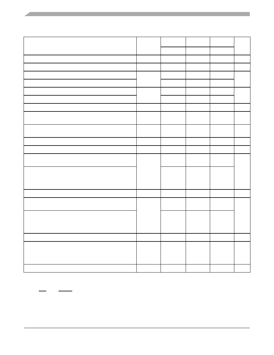
Electrical Characteristics
Freescale Semiconductor
8
(VDD rising)
2.16
2.19
2.27
Power on reset (POR) re-arm voltage
Vpor
—1.4
—
V
Bandgap voltage reference
VBG
1.18
1.20
1.21
V
Input high voltage (VDD > 2.3 V) (all digital inputs)
VIH
0.70
× V
DD
——
V
Input high voltage (1.8 V
≤ V
DD ≤ 2.3 V) (all digital inputs)
0.85
× V
DD
——
Input low voltage (VDD > 2.3 V) (all digital inputs)
VIL
—
0.35
× V
DD
V
Input low voltage (1.8 V
≤ V
DD ≤ 2.3 V) (all digital inputs)
—
0.30
× V
DD
Input hysteresis (all digital inputs)
Vhys
0.06
× V
DD
——
V
Input leakage current (per pin)
VIn = VDD or VSS, all input-only pins
|IIn|
—
0.025
1.0
μA
High impedance (off-state) leakage current (per pin)
VIn = VDD or VSS, all input/output
|IOZ|
—
0.025
1.0
μA
Internal pullup resistors3,4
RPU
17.5
—
52.5
k
Ω
Internal pulldown resistor (KBI)
RPD
17.5
—
52.5
k
Ω
Output high voltage — low drive (PTxDSn = 0)
IOH = –2 mA (VDD ≥ 1.8 V)
VOH
VDD – 0.5
—
V
Output high voltage — high drive (PTxDSn = 1)
IOH = –10 mA (VDD ≥ 2.7 V)
IOH = –6 mA (VDD ≥ 2.3 V)
IOH = –3 mA (VDD ≥ 1.8 V)
VDD – 0.5
—
Maximum total IOH for all port pins
|IOHT|—
—
60
mA
Output low voltage — low drive (PTxDSn = 0)
IOL = 2.0 mA (VDD ≥ 1.8 V)
VOL
——
0.5
V
Output low voltage — high drive (PTxDSn = 1)
IOL = 10.0 mA (VDD ≥ 2.7 V)
IOL = 6 mA (VDD ≥ 2.3 V)
IOL = 3 mA (VDD ≥ 1.8 V)
—
0.5
Maximum total IOL for all port pins
IOLT
——
60
mA
DC injection current 2, 5, 6, 7
VIn < VSS, VIn > VDD
Single pin limit
Total MCU limit, includes sum of all stressed pins
IIC
–0.2
–5
—
0.2
5
mA
Input capacitance (all non-supply pins)
CIn
——
7
pF
1 RAM will retain data down to POR voltage. RAM data not guaranteed to be valid following a POR.
2 This parameter is characterized and not tested on each device.
3 Measurement condition for pull resistors: V
In = VSS for pullup and VIn = VDD for pulldown.
4 PTA5/IRQ/TCLK/RESET pullup resistor may not pull up to the specified minimum V
IH. However, all ports are functionally tested
to guarantee that a logic 1 will be read on any port input when the pullup is enabled and no DC load is present on the pin.
5 All functional non-supply pins are internally clamped to V
SS and VDD.
Table 6. DC Characteristics (Temperature Range = –40 to 85
°C Ambient) (continued)
Parameter
Symbol
Min
Typical
Max
Unit
相关PDF资料 |
PDF描述 |
|---|---|
| ML60851ETB | UNIVERSAL SERIAL BUS CONTROLLER, PQFP44 |
| MPC8555ECVTAKE | RISC PROCESSOR, PBGA783 |
| MB89P485L-104PMC | MICROCONTROLLER, PQFP64 |
| MB88151APNF-G-201-JNE1 | OTHER CLOCK GENERATOR, PDSO8 |
| MCP23018T-E/SS | PIA-GENERAL PURPOSE, PDSO24 |
相关代理商/技术参数 |
参数描述 |
|---|---|
| MC9S08QA2CFQE | 制造商:Freescale Semiconductor 功能描述:IC 8BIT MCU HCS08 20MHZ DFN-8 |
| MC9S08QA2CFQEE | 制造商:FREESCALE 制造商全称:Freescale Semiconductor, Inc 功能描述:Technical Data |
| MC9S08QA2CPAE | 功能描述:8位微控制器 -MCU 9S08QA4 - CI RoHS:否 制造商:Silicon Labs 核心:8051 处理器系列:C8051F39x 数据总线宽度:8 bit 最大时钟频率:50 MHz 程序存储器大小:16 KB 数据 RAM 大小:1 KB 片上 ADC:Yes 工作电源电压:1.8 V to 3.6 V 工作温度范围:- 40 C to + 105 C 封装 / 箱体:QFN-20 安装风格:SMD/SMT |
| MC9S08QA2CPAE | 制造商:Freescale Semiconductor 功能描述:IC 8BIT MCU HCS08 20MHZ DIP-8 |
| MC9S08QA4 | 制造商:FREESCALE 制造商全称:Freescale Semiconductor, Inc 功能描述:8-bit HCS08 Central Processor Unit (CPU) |
发布紧急采购,3分钟左右您将得到回复。