- 您现在的位置:买卖IC网 > PDF目录80581 > MC9S12C96CFA16 (MOTOROLA INC) 16-BIT, FLASH, 16 MHz, MICROCONTROLLER, PQFP48 PDF资料下载
参数资料
| 型号: | MC9S12C96CFA16 |
| 厂商: | MOTOROLA INC |
| 元件分类: | 微控制器/微处理器 |
| 英文描述: | 16-BIT, FLASH, 16 MHz, MICROCONTROLLER, PQFP48 |
| 封装: | LQFP-48 |
| 文件页数: | 105/136页 |
| 文件大小: | 2022K |
| 代理商: | MC9S12C96CFA16 |
第1页第2页第3页第4页第5页第6页第7页第8页第9页第10页第11页第12页第13页第14页第15页第16页第17页第18页第19页第20页第21页第22页第23页第24页第25页第26页第27页第28页第29页第30页第31页第32页第33页第34页第35页第36页第37页第38页第39页第40页第41页第42页第43页第44页第45页第46页第47页第48页第49页第50页第51页第52页第53页第54页第55页第56页第57页第58页第59页第60页第61页第62页第63页第64页第65页第66页第67页第68页第69页第70页第71页第72页第73页第74页第75页第76页第77页第78页第79页第80页第81页第82页第83页第84页第85页第86页第87页第88页第89页第90页第91页第92页第93页第94页第95页第96页第97页第98页第99页第100页第101页第102页第103页第104页当前第105页第106页第107页第108页第109页第110页第111页第112页第113页第114页第115页第116页第117页第118页第119页第120页第121页第122页第123页第124页第125页第126页第127页第128页第129页第130页第131页第132页第133页第134页第135页第136页
Device User Guide — 9S12C128DGV1/D V01.05
70
changed to known start-up states. Refer to the respective module Block User Guides for register reset
states.
5.3.1 Reset Summary Table
5.3.2 Effects of Reset
When a reset occurs, MCU registers and control bits are changed to known start-up states. Refer to the
respective module Block User Guides for register reset states. Refer to the HCS12 Multiplexed External
Bus Interface (MEBI) Block Guide for mode dependent pin configuration of port A, B and E out of reset.
Refer to the PIM Block User Guide for reset configurations of all peripheral module ports.
Refer to Figure 1-2 to Figure 1-5 footnotes for locations of the memories depending on the operating
mode after reset.
The RAM array is not automatically initialized out of reset.
NOTE:
For devices assembled in 48-pin or 52-pin LQFP packages all non-bonded out pins
should be configured as outputs after reset in order to avoid current drawn from
floating inputs. Refer to Table 2-1 for affected pins.
Section 6 HCS12 Core Block Description
Consult the individual block guides for information about the HCS12 core modules, i.e. central processing
unit (CPU), interrupt module (INT), module mapping control module (MMC), multiplexed external bus
interface (MEBI), debug12 module (DBG12) and background debug mode module (BDM).
Where the CPU12 Reference Manual refers to cycles this is equivalent to device bus clock periods.
6.1 Device-specific information
6.1.1 PPAGE
External paging is not supported on these devices. In order to access the 16K flash blocks in the address
range $8000-$BFFF the PPAGE register must be loaded with the corresponding value for this range. Refer
to Table 6-1 for device specific page mapping.
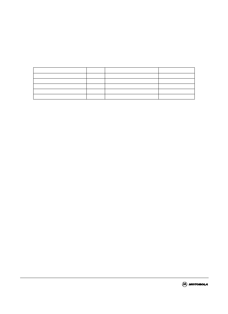
Table 5-2 Reset Summary
Reset
Priority
Source
Vector
Power-on Reset
1
CRG Module
$FFFE, $FFFF
External Reset
1
RESET pin
$FFFE, $FFFF
Low Voltage Reset
1
VREG Module
$FFFE, $FFFF
Clock Monitor Reset
2
CRG Module
$FFFC, $FFFD
COP Watchdog Reset
3
CRG Module
$FFFA, $FFFB
相关PDF资料 |
PDF描述 |
|---|---|
| MC9S12C96PMFU16 | 16-BIT, FLASH, 16 MHz, MICROCONTROLLER, PQFP80 |
| MC9S12GC16CPB25 | 16-BIT, FLASH, 25 MHz, MICROCONTROLLER, PQFP52 |
| M37510M6-XXXFP | 8-BIT, MROM, 4 MHz, MICROCONTROLLER, PQFP176 |
| M926-02I700.0000 | 700 MHz, OTHER CLOCK GENERATOR, CQCC36 |
| MC68HC08GP16AMB | 8-BIT, MROM, 8.2 MHz, MICROCONTROLLER, PDIP42 |
相关代理商/技术参数 |
参数描述 |
|---|---|
| MC9S12C96CFAE | 功能描述:16位微控制器 - MCU 9S12C96-KOI-EPP RoHS:否 制造商:Texas Instruments 核心:RISC 处理器系列:MSP430FR572x 数据总线宽度:16 bit 最大时钟频率:24 MHz 程序存储器大小:8 KB 数据 RAM 大小:1 KB 片上 ADC:Yes 工作电源电压:2 V to 3.6 V 工作温度范围:- 40 C to + 85 C 封装 / 箱体:VQFN-40 安装风格:SMD/SMT |
| MC9S12C96CFU | 制造商:Freescale Semiconductor 功能描述:16-BIT, FLASH, 25 MHz, MICROCONTROLLER, PQFP80 |
| MC9S12C96CFUE | 功能描述:16位微控制器 - MCU 9S12C96 (KOI) - PB FREE RoHS:否 制造商:Texas Instruments 核心:RISC 处理器系列:MSP430FR572x 数据总线宽度:16 bit 最大时钟频率:24 MHz 程序存储器大小:8 KB 数据 RAM 大小:1 KB 片上 ADC:Yes 工作电源电压:2 V to 3.6 V 工作温度范围:- 40 C to + 85 C 封装 / 箱体:VQFN-40 安装风格:SMD/SMT |
| MC9S12C96CFUER | 功能描述:16位微控制器 - MCU 9S12C96 (KOI) - PB FREE RoHS:否 制造商:Texas Instruments 核心:RISC 处理器系列:MSP430FR572x 数据总线宽度:16 bit 最大时钟频率:24 MHz 程序存储器大小:8 KB 数据 RAM 大小:1 KB 片上 ADC:Yes 工作电源电压:2 V to 3.6 V 工作温度范围:- 40 C to + 85 C 封装 / 箱体:VQFN-40 安装风格:SMD/SMT |
| MC9S12C96CPBE | 功能描述:16位微控制器 - MCU 9S12C96 TSMC3 EPP RoHS:否 制造商:Texas Instruments 核心:RISC 处理器系列:MSP430FR572x 数据总线宽度:16 bit 最大时钟频率:24 MHz 程序存储器大小:8 KB 数据 RAM 大小:1 KB 片上 ADC:Yes 工作电源电压:2 V to 3.6 V 工作温度范围:- 40 C to + 85 C 封装 / 箱体:VQFN-40 安装风格:SMD/SMT |
发布紧急采购,3分钟左右您将得到回复。