- 您现在的位置:买卖IC网 > PDF目录45295 > MC9S12C96MFA16 (MOTOROLA INC) 16-BIT, FLASH, 16 MHz, MICROCONTROLLER, PQFP48 PDF资料下载
参数资料
| 型号: | MC9S12C96MFA16 |
| 厂商: | MOTOROLA INC |
| 元件分类: | 微控制器/微处理器 |
| 英文描述: | 16-BIT, FLASH, 16 MHz, MICROCONTROLLER, PQFP48 |
| 封装: | LQFP-48 |
| 文件页数: | 98/136页 |
| 文件大小: | 2022K |
| 代理商: | MC9S12C96MFA16 |
第1页第2页第3页第4页第5页第6页第7页第8页第9页第10页第11页第12页第13页第14页第15页第16页第17页第18页第19页第20页第21页第22页第23页第24页第25页第26页第27页第28页第29页第30页第31页第32页第33页第34页第35页第36页第37页第38页第39页第40页第41页第42页第43页第44页第45页第46页第47页第48页第49页第50页第51页第52页第53页第54页第55页第56页第57页第58页第59页第60页第61页第62页第63页第64页第65页第66页第67页第68页第69页第70页第71页第72页第73页第74页第75页第76页第77页第78页第79页第80页第81页第82页第83页第84页第85页第86页第87页第88页第89页第90页第91页第92页第93页第94页第95页第96页第97页当前第98页第99页第100页第101页第102页第103页第104页第105页第106页第107页第108页第109页第110页第111页第112页第113页第114页第115页第116页第117页第118页第119页第120页第121页第122页第123页第124页第125页第126页第127页第128页第129页第130页第131页第132页第133页第134页第135页第136页
Device User Guide — 9S12C128DGV1/D V01.05
64
2.4.4 VDDA, VSSA — Power Supply Pins for ATD and VREG
VDDA, VSSA are the power supply and ground input pins for the voltage regulator reference and the
analog to digital converter.
2.4.5 VRH, VRL — ATD Reference Voltage Input Pins
VRH and VRL are the reference voltage input pins for the analog to digital converter.
2.4.6 VDDPLL, VSSPLL — Power Supply Pins for PLL
Provides operating voltage and ground for the Oscillator and the Phased-Locked Loop. This allows the
supply voltage to the Oscillator and PLL to be bypassed independently. This 2.5V voltage is generated by
the internal voltage regulator.
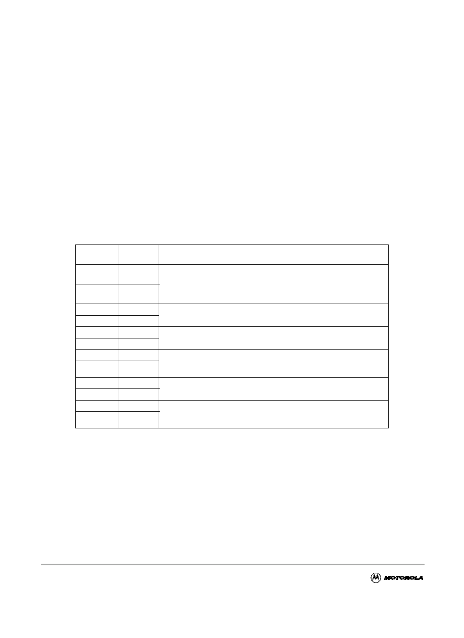
Table 2-2 MC9S12C-Family Power and Ground Connection Summary
NOTE:All VSS pins must be connected together in the application. Because fast signal transitions
place high, short-duration current demands on the power supply, use bypass capacitors with
high-frequency characteristics and place them as close to the MCU as possible. Bypass requirements
depend on MCU pin load.
Section 3 System Clock Description
Mnemonic
Nominal
Voltage
Description
VDD1
VDD2
2.5 V
Internal power and ground generated by internal regulator. These also
allow an external source to supply the core VDD/VSS voltages and bypass
the internal voltage regulator.
In the 48 and 52 LQFP packages VDD2 and VSS2 are not available.
VSS1
VSS2
0V
VDDR
5.0 V
External power and ground, supply to internal voltage regulator.
VSSR
0 V
VDDX
5.0 V
External power and ground, supply to pin drivers.
VSSX
0 V
VDDA
5.0 V
Operating voltage and ground for the analog-to-digital converters and the
reference for the internal voltage regulator, allows the supply voltage to the
A/D to be bypassed independently.
VSSA
0 V
VRH
5.0 V
Reference voltage low for the ATD converter.
In the 48 and 52 LQFP packages VRL is bonded to VSSA.
VRL
0 V
VDDPLL
2.5 V
Provides operating voltage and ground for the Phased-Locked Loop. This
allows the supply voltage to the PLL to be bypassed independently.
Internal power and ground generated by internal regulator.
VSSPLL
0 V
相关PDF资料 |
PDF描述 |
|---|---|
| MC9S12C128CFA25 | 16-BIT, FLASH, 25 MHz, MICROCONTROLLER, PQFP48 |
| MC9S12C128CFU16 | 16-BIT, FLASH, 16 MHz, MICROCONTROLLER, PQFP80 |
| MC9S12GC32CPB25 | 16-BIT, FLASH, 25 MHz, MICROCONTROLLER, PQFP52 |
| MC9S12GC32VFU25 | 16-BIT, FLASH, 25 MHz, MICROCONTROLLER, PQFP80 |
| MC9S12C32MFA25 | 16-BIT, FLASH, 25 MHz, MICROCONTROLLER, PQFP48 |
相关代理商/技术参数 |
参数描述 |
|---|---|
| MC9S12C96MFAE | 功能描述:16位微控制器 - MCU 9S12C96 (KOI) RoHS:否 制造商:Texas Instruments 核心:RISC 处理器系列:MSP430FR572x 数据总线宽度:16 bit 最大时钟频率:24 MHz 程序存储器大小:8 KB 数据 RAM 大小:1 KB 片上 ADC:Yes 工作电源电压:2 V to 3.6 V 工作温度范围:- 40 C to + 85 C 封装 / 箱体:VQFN-40 安装风格:SMD/SMT |
| MC9S12C96MFUE | 功能描述:16位微控制器 - MCU 9S12C96 (KOI) RoHS:否 制造商:Texas Instruments 核心:RISC 处理器系列:MSP430FR572x 数据总线宽度:16 bit 最大时钟频率:24 MHz 程序存储器大小:8 KB 数据 RAM 大小:1 KB 片上 ADC:Yes 工作电源电压:2 V to 3.6 V 工作温度范围:- 40 C to + 85 C 封装 / 箱体:VQFN-40 安装风格:SMD/SMT |
| MC9S12C96MPBE | 功能描述:IC MCU 96K FLASH 4K RAM 52-LQFP RoHS:否 类别:集成电路 (IC) >> 嵌入式 - 微控制器, 系列:HCS12 标准包装:330 系列:- 核心处理器:- 芯体尺寸:8/16-位 速度:40MHz 连通性:UART/USART 外围设备:DMA,PWM,WDT 输入/输出数:32 程序存储器容量:- 程序存储器类型:外部程序存储器 EEPROM 大小:- RAM 容量:- 电压 - 电源 (Vcc/Vdd):4.5 V ~ 5.5 V 数据转换器:- 振荡器型:内部 工作温度:-40°C ~ 85°C 封装/外壳:100-BQFP 包装:管件 |
| MC9S12C96MPBER | 功能描述:IC MCU 96K FLASH 4K RAM 52-LQFP RoHS:是 类别:集成电路 (IC) >> 嵌入式 - 微控制器, 系列:HCS12 标准包装:1 系列:87C 核心处理器:MCS 51 芯体尺寸:8-位 速度:16MHz 连通性:SIO 外围设备:- 输入/输出数:32 程序存储器容量:8KB(8K x 8) 程序存储器类型:OTP EEPROM 大小:- RAM 容量:256 x 8 电压 - 电源 (Vcc/Vdd):4 V ~ 6 V 数据转换器:- 振荡器型:外部 工作温度:0°C ~ 70°C 封装/外壳:44-DIP 包装:管件 其它名称:864285 |
| MC9S12C96VFAE | 功能描述:IC MCU 96K FLASH 4K RAM 48-LQFP RoHS:是 类别:集成电路 (IC) >> 嵌入式 - 微控制器, 系列:HCS12 标准包装:1 系列:87C 核心处理器:MCS 51 芯体尺寸:8-位 速度:16MHz 连通性:SIO 外围设备:- 输入/输出数:32 程序存储器容量:8KB(8K x 8) 程序存储器类型:OTP EEPROM 大小:- RAM 容量:256 x 8 电压 - 电源 (Vcc/Vdd):4 V ~ 6 V 数据转换器:- 振荡器型:外部 工作温度:0°C ~ 70°C 封装/外壳:44-DIP 包装:管件 其它名称:864285 |
发布紧急采购,3分钟左右您将得到回复。