- 您现在的位置:买卖IC网 > PDF目录359659 > MCF5213 (飞思卡尔半导体(中国)有限公司) ColdFire Microcontroller PDF资料下载
参数资料
| 型号: | MCF5213 |
| 厂商: | 飞思卡尔半导体(中国)有限公司 |
| 英文描述: | ColdFire Microcontroller |
| 中文描述: | ColdFire微控制器 |
| 文件页数: | 29/56页 |
| 文件大小: | 608K |
| 代理商: | MCF5213 |
第1页第2页第3页第4页第5页第6页第7页第8页第9页第10页第11页第12页第13页第14页第15页第16页第17页第18页第19页第20页第21页第22页第23页第24页第25页第26页第27页第28页当前第29页第30页第31页第32页第33页第34页第35页第36页第37页第38页第39页第40页第41页第42页第43页第44页第45页第46页第47页第48页第49页第50页第51页第52页第53页第54页第55页第56页
Electrical Characteristics
MCF5213 ColdFire Microcontroller, Rev. 3
Freescale Semiconductor
29
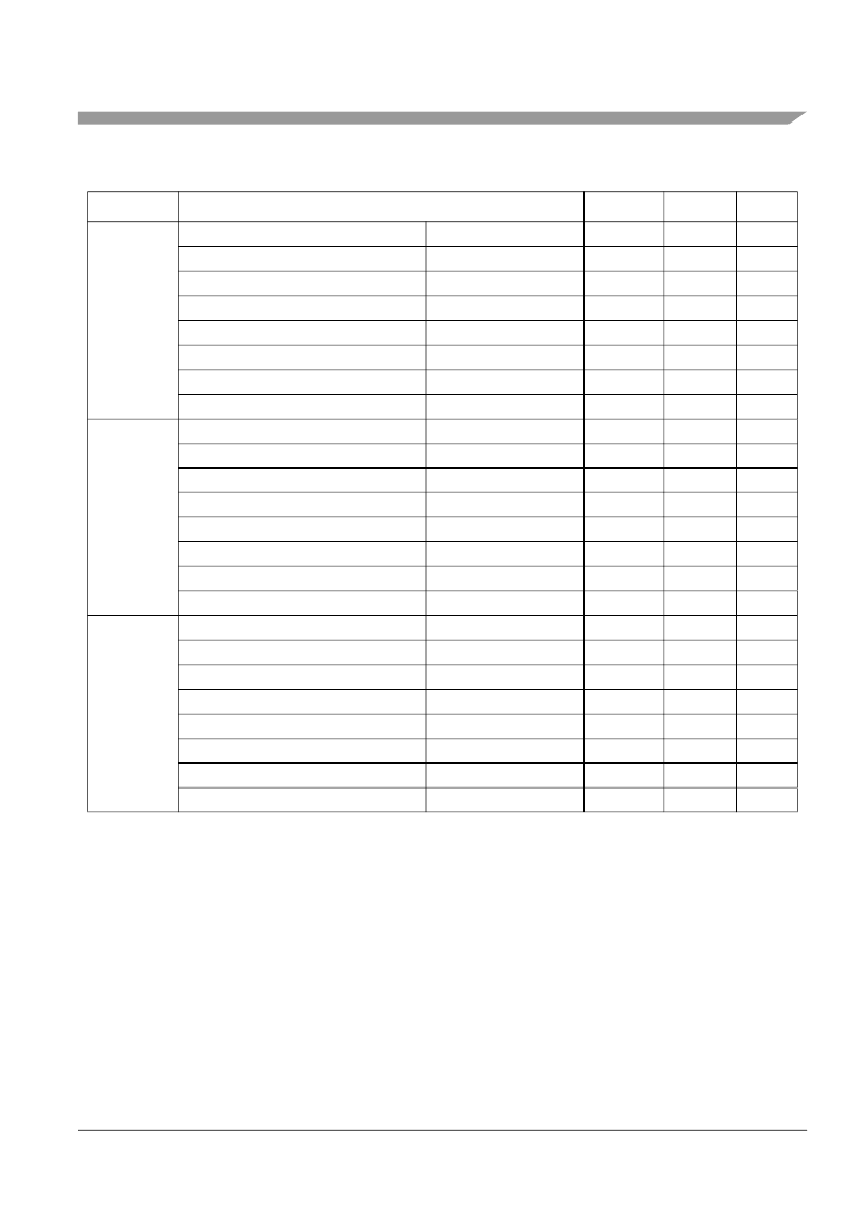
81 MAPBGA Junction to ambient, natural convection
Single layer board (1s)
θ
JA
θ
JA
θ
JMA
θ
JMA
θ
JB
θ
JC
Ψ
jt
61
1,2
°
C / W
Junction to ambient, natural convection
Four layer board (2s2p)
35
2,3
°
C / W
Junction to ambient, (@200 ft/min)
Single layer board (1s)
50
2,3
°
C / W
Junction to ambient, (@200 ft/min)
Four layer board (2s2p)
31
2,3
°
C / W
Junction to board
—
20
4
°
C / W
Junction to case
—
12
5
°
C / W
Junction to top of package
Natural convection
2
6
°
C / W
Maximum operating junction temperature
—
T
j
θ
JA
θ
JA
θ
JMA
θ
JMA
θ
JB
θ
JC
Ψ
jt
105
o
C
64 LQFP
Junction to ambient, natural convection
Single layer board (1s)
62
1,2
°
C / W
Junction to ambient, natural convection
Four layer board (2s2p)
43
1,3
°
C / W
Junction to ambient (@200 ft/min)
Single layer board (1s)
50
1,3
°
C / W
Junction to ambient (@200 ft/min)
Four layer board (2s2p)
36
1,3
°
C / W
Junction to board
—
26
4
°
C / W
Junction to case
—
9
5
°
C / W
Junction to top of package
Natural convection
2
6
°
C / W
Maximum operating junction temperature
—
T
j
θ
JA
θ
JA
θ
JMA
θ
JMA
θ
JB
θ
JC
Ψ
jt
105
o
C
64 QFN
Junction to ambient, natural convection
Single layer board (1s)
68
1,2
°
C / W
Junction to ambient, natural convection
Four layer board (2s2p)
24
1,3
°
C / W
Junction to ambient (@200 ft/min)
Single layer board (1s)
55
1,3
°
C / W
Junction to ambient (@200 ft/min)
Four layer board (2s2p)
19
1,3
°
C / W
Junction to board
—
8
4
°
C / W
Junction to case (bottom)
—
0.6
5
°
C / W
Junction to top of package
Natural convection
3
6
°
C / W
Maximum operating junction temperature
—
T
j
105
o
C
1
θ
JA
and
Ψ
jt
parameters are simulated in conformance with EIA/JESD Standard 51-2 for natural convection. Freescale
recommends the use of
θ
JA
and power dissipation specifications in the system design to prevent device junction
temperatures from exceeding the rated specification. System designers should be aware that device junction temperatures
can be significantly influenced by board layout and surrounding devices. Conformance to the device junction temperature
specification can be verified by physical measurement in the customer’s system using the
Ψ
jt
parameter, the device power
dissipation, and the method described in EIA/JESD Standard 51-2.
2
Per JEDEC JESD51-2 with the single-layer board (JESD51-3) horizontal.
3
Per JEDEC JESD51-6 with the board JESD51-7) horizontal.
4
Thermal resistance between the die and the printed circuit board in conformance with JEDEC JESD51-8. Board
temperature is measured on the top surface of the board near the package.
5
Thermal resistance between the die and the case top surface as measured by the cold plate method (MIL SPEC-883
Method 1012.1).
6
Thermal characterization parameter indicating the temperature difference between package top and the junction
temperature per JEDEC JESD51-2. When Greek letters are not available, the thermal characterization parameter is written
in conformance with Psi-JT.
Table 22. Thermal Characteristics (continued)
Characteristic
Symbol
Value
Unit
相关PDF资料 |
PDF描述 |
|---|---|
| MCF5213_07 | ColdFire Microcontroller |
| MCF5213CAF66 | ColdFire Microcontroller |
| MCF5213CAF80 | ColdFire Microcontroller |
| MCF5213LCVM66 | ColdFire Microcontroller |
| MCF5213LCVM80 | ColdFire Microcontroller |
相关代理商/技术参数 |
参数描述 |
|---|---|
| MCF5213_07 | 制造商:FREESCALE 制造商全称:Freescale Semiconductor, Inc 功能描述:ColdFire Microcontroller |
| MCF5213_10 | 制造商:FREESCALE 制造商全称:Freescale Semiconductor, Inc 功能描述:MCF5213 ColdFire Microcontroller |
| MCF5213CAF66 | 功能描述:32位微控制器 - MCU MCF5213 KIRIN RoHS:否 制造商:Texas Instruments 核心:C28x 处理器系列:TMS320F28x 数据总线宽度:32 bit 最大时钟频率:90 MHz 程序存储器大小:64 KB 数据 RAM 大小:26 KB 片上 ADC:Yes 工作电源电压:2.97 V to 3.63 V 工作温度范围:- 40 C to + 105 C 封装 / 箱体:LQFP-80 安装风格:SMD/SMT |
| MCF5213CAF80 | 功能描述:32位微控制器 - MCU MCF5213 KIRIN RoHS:否 制造商:Texas Instruments 核心:C28x 处理器系列:TMS320F28x 数据总线宽度:32 bit 最大时钟频率:90 MHz 程序存储器大小:64 KB 数据 RAM 大小:26 KB 片上 ADC:Yes 工作电源电压:2.97 V to 3.63 V 工作温度范围:- 40 C to + 105 C 封装 / 箱体:LQFP-80 安装风格:SMD/SMT |
| MCF5213LCVM66 | 功能描述:32位微控制器 - MCU MCF5213 KIRIN RoHS:否 制造商:Texas Instruments 核心:C28x 处理器系列:TMS320F28x 数据总线宽度:32 bit 最大时钟频率:90 MHz 程序存储器大小:64 KB 数据 RAM 大小:26 KB 片上 ADC:Yes 工作电源电压:2.97 V to 3.63 V 工作温度范围:- 40 C to + 105 C 封装 / 箱体:LQFP-80 安装风格:SMD/SMT |
发布紧急采购,3分钟左右您将得到回复。