- 您现在的位置:买卖IC网 > PDF目录69032 > MCF5235CVM150 (FREESCALE SEMICONDUCTOR INC) 32-BIT, 150 MHz, RISC PROCESSOR, PBGA256 PDF资料下载
参数资料
| 型号: | MCF5235CVM150 |
| 厂商: | FREESCALE SEMICONDUCTOR INC |
| 元件分类: | 微控制器/微处理器 |
| 英文描述: | 32-BIT, 150 MHz, RISC PROCESSOR, PBGA256 |
| 封装: | ROHS COMPLIANT, MAPBGA-256 |
| 文件页数: | 19/48页 |
| 文件大小: | 666K |
| 代理商: | MCF5235CVM150 |
第1页第2页第3页第4页第5页第6页第7页第8页第9页第10页第11页第12页第13页第14页第15页第16页第17页第18页当前第19页第20页第21页第22页第23页第24页第25页第26页第27页第28页第29页第30页第31页第32页第33页第34页第35页第36页第37页第38页第39页第40页第41页第42页第43页第44页第45页第46页第47页第48页
MCF523x Integrated Microprocessor Hardware Specification, Rev. 4
Electrical Characteristics
Freescale Semiconductor
26
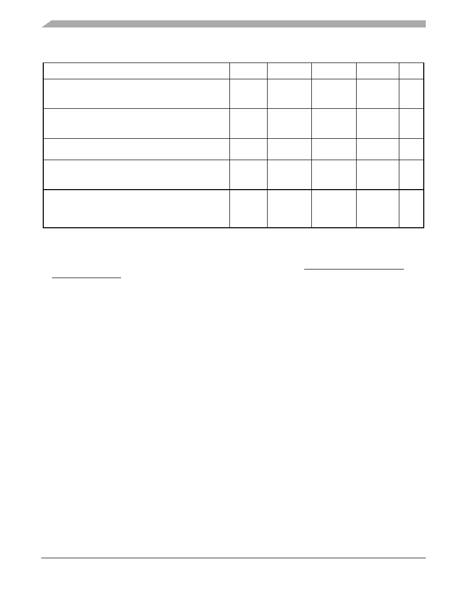
Input Capacitance 3
All input-only pins
All input/output (three-state) pins
Cin
—
7
pF
Load Capacitance4
Low drive strength
High drive strength
CL
—
25
50
pF
Core Operating Supply Current 5
Master Mode
IDD
—
135
150
mA
Pad Operating Supply Current
Master Mode
Low Power Modes
OIDD
—
100
TBD
—
mA
μA
DC Injection Current 3, 6, 7, 8
VNEGCLAMP =VSS– 0.3 V, VPOSCLAMP = VDD + 0.3
Single Pin Limit
Total processor Limit, Includes sum of all stressed pins
IIC
–1.0
–10
1.0
10
mA
1
Refer to Table 10 for additional PLL specifications.
2
Refer to the MCF5235 signals section for pins having weak internal pull-up devices.
3
This parameter is characterized before qualification rather than 100% tested.
4
pF load ratings are based on DC loading and are provided as an indication of driver strength. High speed interfaces require
transmission line analysis to determine proper drive strength and termination. See High Speed Signal Propagation:
Advanced Black Magic by Howard W. Johnson for design guidelines.
5
Current measured at maximum system clock frequency, all modules active, and default drive strength with matching load.
6
All functional non-supply pins are internally clamped to VSS and their respective VDD.
7
Input must be current limited to the value specified. To determine the value of the required current-limiting resistor, calculate
resistance values for positive and negative clamp voltages, then use the larger of the two values.
8
Power supply must maintain regulation within operating VDD range during instantaneous and operating maximum current
conditions. If positive injection current (Vin > VDD) is greater than IDD, the injection current may flow out of VDD and could
result in external power supply going out of regulation. Insure external VDD load will shunt current greater than maximum
injection current. This will be the greatest risk when the processor is not consuming power. Examples are: if no system
clock is present, or if clock rate is very low which would reduce overall power consumption. Also, at power-up, system clock
is not present during the power-up sequence until the PLL has attained lock.
Table 9. DC Electrical Specifications1 (continued)
Characteristic
Symbol
Min
Typical
Max
Unit
相关PDF资料 |
PDF描述 |
|---|---|
| MCF5235CVF150 | 32-BIT, 150 MHz, RISC PROCESSOR, PBGA256 |
| MCF5249CVF140 | 32-BIT, 140 MHz, RISC PROCESSOR, PBGA160 |
| MCF5249VM140 | 32-BIT, 140 MHz, RISC PROCESSOR, PBGA160 |
| MCF5249VF140 | 32-BIT, 140 MHz, RISC PROCESSOR, PBGA160 |
| MCF5251CDVM140 | 32-BIT, 140 MHz, MICROPROCESSOR, PBGA225 |
相关代理商/技术参数 |
参数描述 |
|---|---|
| MCF5235CVM150 | 制造商:Freescale Semiconductor 功能描述:Microprocessor IC |
| MCF5235CVM150J | 功能描述:32位微控制器 - MCU V2CORE 64KSRAM RoHS:否 制造商:Texas Instruments 核心:C28x 处理器系列:TMS320F28x 数据总线宽度:32 bit 最大时钟频率:90 MHz 程序存储器大小:64 KB 数据 RAM 大小:26 KB 片上 ADC:Yes 工作电源电压:2.97 V to 3.63 V 工作温度范围:- 40 C to + 105 C 封装 / 箱体:LQFP-80 安装风格:SMD/SMT |
| MCF5235CVM150J | 制造商:Freescale Semiconductor 功能描述:IC 32-BIT MPU 150 MHz 256-BGA |
| MCF5235EC | 制造商:FREESCALE 制造商全称:Freescale Semiconductor, Inc 功能描述:Integrated Microprocessor Hardware Specification |
| MCF523X | 制造商:FREESCALE 制造商全称:Freescale Semiconductor, Inc 功能描述:Integrated Microprocessor Hardware Specification |
发布紧急采购,3分钟左右您将得到回复。