- 您现在的位置:买卖IC网 > PDF目录10955 > MCF5327CVM240 (Freescale Semiconductor)IC MPU RISC 240MHZ 196-MAPBGA PDF资料下载
参数资料
| 型号: | MCF5327CVM240 |
| 厂商: | Freescale Semiconductor |
| 文件页数: | 14/50页 |
| 文件大小: | 0K |
| 描述: | IC MPU RISC 240MHZ 196-MAPBGA |
| 标准包装: | 126 |
| 系列: | MCF532x |
| 核心处理器: | Coldfire V3 |
| 芯体尺寸: | 32-位 |
| 速度: | 240MHz |
| 连通性: | EBI/EMI,I²C,SPI,SSI,UART/USART,USB,USB OTG |
| 外围设备: | DMA,LCD,PWM,WDT |
| 输入/输出数: | 94 |
| 程序存储器类型: | ROMless |
| RAM 容量: | 32K x 8 |
| 电压 - 电源 (Vcc/Vdd): | 1.4 V ~ 3.6 V |
| 振荡器型: | 外部 |
| 工作温度: | -40°C ~ 85°C |
| 封装/外壳: | 196-LBGA |
| 包装: | 托盘 |
第1页第2页第3页第4页第5页第6页第7页第8页第9页第10页第11页第12页第13页当前第14页第15页第16页第17页第18页第19页第20页第21页第22页第23页第24页第25页第26页第27页第28页第29页第30页第31页第32页第33页第34页第35页第36页第37页第38页第39页第40页第41页第42页第43页第44页第45页第46页第47页第48页第49页第50页
Electrical Characteristics
MCF532x ColdFire Microprocessor Data Sheet, Rev. 5
Freescale Semiconductor
21
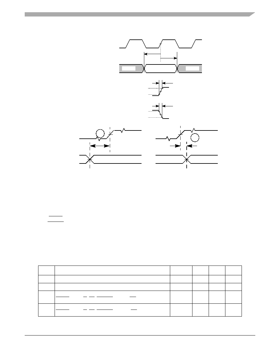
Figure 6. General Input Timing Requirements
5.6.1
FlexBus
A multi-function external bus interface called FlexBus is provided with basic functionality to interface to slave-only devices up
to a maximum bus frequency of 80MHz. It can be directly connected to asynchronous or synchronous devices such as external
boot ROMs, flash memories, gate-array logic, or other simple target (slave) devices with little or no additional circuitry. For
asynchronous devices a simple chip-select based interface can be used. The FlexBus interface has six general purpose
chip-selects (FB_CS[5:0]) which can be configured to be distributed between the FlexBus or SDRAM memory interfaces.
Chip-select, FB_CS0 can be dedicated to boot ROM access and can be programmed to be byte (8 bits), word (16 bits), or
longword (32 bits) wide. Control signal timing is compatible with common ROM/flash memories.
5.6.1.1
FlexBus AC Timing Characteristics
The following timing numbers indicate when data is latched or driven onto the external bus, relative to the system clock.
Table 9. FlexBus AC Timing Specifications
Num
Characteristic
Symbol
Min
Max
Unit
—
Frequency of Operation
fsys/3
—80
Mhz
FB1
Clock Period (FB_CLK)
tFBCK (tcyc)
12.5
—
ns
FB2
Address, Data, and Control Output Valid (A[23:0], D[31:0],
FB_CS[5:0], R/W, TS, BE/BWE[3:0] and OE)1
tFBCHDCV
—7.0
ns
FB3
Address, Data, and Control Output Hold (A[23:0], D[31:0],
FB_CS[5:0], R/W, TS, BE/BWE[3:0], and OE)1, 2
tFBCHDCI
1—
ns
Invalid
FB_CLK (80MHz)
TSETUP
THOLD
Input Setup And Hold
1.5V
trise
Vh = VIH
Vl = VIL
1.5V
1.5V Valid
tfall
Vh = VIH
Vl = VIL
Input Rise Time
Input Fall Time
* The timings are also valid for inputs sampled on the negative clock edge.
Inputs
FB_CLK
B4
B5
相关PDF资料 |
PDF描述 |
|---|---|
| VE-B7R-IW-B1 | CONVERTER MOD DC/DC 7.5V 100W |
| MC9S12C96MFAE | IC MCU 96K FLASH 4K RAM 48-LQFP |
| VE-B6W-IW-B1 | CONVERTER MOD DC/DC 5.5V 100W |
| MC9S12XDT256CAG | IC MCU 256K FLASH 144-LQFP |
| MC9S12C96MFUE | IC MCU 96K FLASH 4K RAM 80-QFP |
相关代理商/技术参数 |
参数描述 |
|---|---|
| MCF5327CVM240J | 制造商:Freescale Semiconductor 功能描述:MPC5XXX RISC 32-BIT CMOS 240MHZ 196-PIN MA-BGA TRAY - Trays |
| MCF5328 | 制造商:FREESCALE 制造商全称:Freescale Semiconductor, Inc 功能描述:ColdFire㈢ Microprocessor |
| MCF53281 | 制造商:FREESCALE 制造商全称:Freescale Semiconductor, Inc 功能描述:ColdFire㈢ Microprocessor |
| MCF53281CVM240 | 功能描述:微处理器 - MPU MCF5329 DRAGONFIRE RoHS:否 制造商:Atmel 处理器系列:SAMA5D31 核心:ARM Cortex A5 数据总线宽度:32 bit 最大时钟频率:536 MHz 程序存储器大小:32 KB 数据 RAM 大小:128 KB 接口类型:CAN, Ethernet, LIN, SPI,TWI, UART, USB 工作电源电压:1.8 V to 3.3 V 最大工作温度:+ 85 C 安装风格:SMD/SMT 封装 / 箱体:FBGA-324 |
| MCF53281CVM240J | 功能描述:32位微控制器 - MCU DRAGONFIRE RoHS:否 制造商:Texas Instruments 核心:C28x 处理器系列:TMS320F28x 数据总线宽度:32 bit 最大时钟频率:90 MHz 程序存储器大小:64 KB 数据 RAM 大小:26 KB 片上 ADC:Yes 工作电源电压:2.97 V to 3.63 V 工作温度范围:- 40 C to + 105 C 封装 / 箱体:LQFP-80 安装风格:SMD/SMT |
发布紧急采购,3分钟左右您将得到回复。