- 您现在的位置:买卖IC网 > PDF目录10937 > MCF5328CVM240J (Freescale Semiconductor)IC MPU RISC 240MHZ 256MAPBGA PDF资料下载
参数资料
| 型号: | MCF5328CVM240J |
| 厂商: | Freescale Semiconductor |
| 文件页数: | 19/50页 |
| 文件大小: | 0K |
| 描述: | IC MPU RISC 240MHZ 256MAPBGA |
| 标准包装: | 90 |
| 系列: | MCF532x |
| 核心处理器: | Coldfire V3 |
| 芯体尺寸: | 32-位 |
| 速度: | 240MHz |
| 连通性: | EBI/EMI,以太网,I²C,SPI,SSI,UART/USART,USB,USB OTG |
| 外围设备: | DMA,LCD,PWM,WDT |
| 输入/输出数: | 94 |
| 程序存储器类型: | ROMless |
| RAM 容量: | 32K x 8 |
| 电压 - 电源 (Vcc/Vdd): | 1.4 V ~ 3.6 V |
| 振荡器型: | 外部 |
| 工作温度: | -40°C ~ 85°C |
| 封装/外壳: | 256-LBGA |
| 包装: | 托盘 |
第1页第2页第3页第4页第5页第6页第7页第8页第9页第10页第11页第12页第13页第14页第15页第16页第17页第18页当前第19页第20页第21页第22页第23页第24页第25页第26页第27页第28页第29页第30页第31页第32页第33页第34页第35页第36页第37页第38页第39页第40页第41页第42页第43页第44页第45页第46页第47页第48页第49页第50页
MCF532x ColdFire Microprocessor Data Sheet, Rev. 5
Electrical Characteristics
Freescale Semiconductor
26
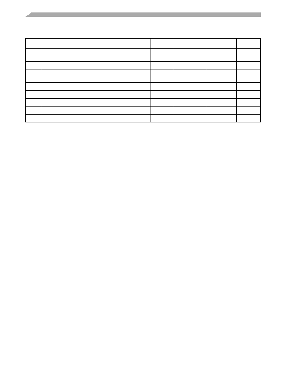
DD8
Data and Data Mask Output Hold (DQS-->DQ) Relative to
DQS (DDR Write Mode)6
tDQDMI
1.0
—
ns
DD9
Input Data Skew Relative to DQS (Input Setup)7
tDVDQ
—1
ns
DD10
Input Data Hold Relative to DQS8
tDIDQ
0.25
× SD_CLK
+0.5ns
—ns
DD11 DQS falling edge from SDCLK rising (output hold time)
tDQLSDCH
0.5
—
ns
DD12 DQS input read preamble width
tDQRPRE
0.9
1.1
SD_CLK
DD13 DQS input read postamble width
tDQRPST
0.4
0.6
SD_CLK
DD14 DQS output write preamble width
tDQWPRE
0.25
SD_CLK
DD15 DQS output write postamble width
tDQWPST
0.4
0.6
SD_CLK
1 SD_CLK is one SDRAM clock in (ns).
2 Pulse width high plus pulse width low cannot exceed min and max clock period.
3 Command output valid should be 1/2 the memory bus clock (SD_CLK) plus some minor adjustments for process, temperature,
and voltage variations.
4 This specification relates to the required input setup time of today’s DDR memories. The processor’s output setup should be
larger than the input setup of the DDR memories. If it is not larger, the input setup on the memory is in violation.
MEM_DATA[31:24] is relative to MEM_DQS[3], MEM_DATA[23:16] is relative to MEM_DQS[2], MEM_DATA[15:8] is relative to
MEM_DQS[1], and MEM_[7:0] is relative MEM_DQS[0].
5 The first data beat is valid before the first rising edge of DQS and after the DQS write preamble. The remaining data beats are
valid for each subsequent DQS edge.
6 This specification relates to the required hold time of today’s DDR memories. MEM_DATA[31:24] is relative to MEM_DQS[3],
MEM_DATA[23:16] is relative to MEM_DQS[2], MEM_DATA[15:8] is relative to MEM_DQS[1], and MEM_[7:0] is relative
MEM_DQS[0].
7 Data input skew is derived from each DQS clock edge. It begins with a DQS transition and ends when the last data line
becomes valid. This input skew must include DDR memory output skew and system level board skew (due to routing or other
factors).
8 Data input hold is derived from each DQS clock edge. It begins with a DQS transition and ends when the first data line
becomes invalid.
Table 11. DDR Timing Specifications (continued)
Num
Characteristic
Symbol
Min
Max
Unit
相关PDF资料 |
PDF描述 |
|---|---|
| MCF5328CVM240 | IC MCU 32BIT 240MHZ 256-MAPBGA |
| VI-23V-CU | CONVERTER MOD DC/DC 5.8V 200W |
| MC9328MX1DVM15R2 | IC MCU I.MX 150MHZ 256-MAPBGA |
| MC912D60CCPVE | IC MCU 16BIT 112-LQFP |
| MCF5280CVM66J | IC MPU RISC 66MHZ 256-MAPBGA |
相关代理商/技术参数 |
参数描述 |
|---|---|
| MCF5329 | 制造商:FREESCALE 制造商全称:Freescale Semiconductor, Inc 功能描述:ColdFire㈢ Microprocessor |
| MCF5329_08 | 制造商:FREESCALE 制造商全称:Freescale Semiconductor, Inc 功能描述:ColdFire㈢ Microprocessor |
| MCF5329CVM240 | 功能描述:IC MCU 32BIT 240MHZ 256-MAPBGA RoHS:是 类别:集成电路 (IC) >> 嵌入式 - 微控制器, 系列:MCF532x 标准包装:330 系列:- 核心处理器:- 芯体尺寸:8/16-位 速度:40MHz 连通性:UART/USART 外围设备:DMA,PWM,WDT 输入/输出数:32 程序存储器容量:- 程序存储器类型:外部程序存储器 EEPROM 大小:- RAM 容量:- 电压 - 电源 (Vcc/Vdd):4.5 V ~ 5.5 V 数据转换器:- 振荡器型:内部 工作温度:-40°C ~ 85°C 封装/外壳:100-BQFP 包装:管件 |
| MCF5329CVM240J | 功能描述:32位微控制器 - MCU V3CORE RoHS:否 制造商:Texas Instruments 核心:C28x 处理器系列:TMS320F28x 数据总线宽度:32 bit 最大时钟频率:90 MHz 程序存储器大小:64 KB 数据 RAM 大小:26 KB 片上 ADC:Yes 工作电源电压:2.97 V to 3.63 V 工作温度范围:- 40 C to + 105 C 封装 / 箱体:LQFP-80 安装风格:SMD/SMT |
| MCF5329DS | 制造商:ANALOGICTECH 制造商全称:Advanced Analogic Technologies 功能描述:MCF5329 ColdFire Microprocessor Data Sheet |
发布紧急采购,3分钟左右您将得到回复。