- 您现在的位置:买卖IC网 > PDF目录45312 > MCF5372LCVM240 (FREESCALE SEMICONDUCTOR INC) 32-BIT, 240 MHz, RISC PROCESSOR, PBGA196 PDF资料下载
参数资料
| 型号: | MCF5372LCVM240 |
| 厂商: | FREESCALE SEMICONDUCTOR INC |
| 元件分类: | 微控制器/微处理器 |
| 英文描述: | 32-BIT, 240 MHz, RISC PROCESSOR, PBGA196 |
| 封装: | 15 X 15 MM, ROHS COMPLIANT, MAPBGA-196 |
| 文件页数: | 15/46页 |
| 文件大小: | 922K |
| 代理商: | MCF5372LCVM240 |
第1页第2页第3页第4页第5页第6页第7页第8页第9页第10页第11页第12页第13页第14页当前第15页第16页第17页第18页第19页第20页第21页第22页第23页第24页第25页第26页第27页第28页第29页第30页第31页第32页第33页第34页第35页第36页第37页第38页第39页第40页第41页第42页第43页第44页第45页第46页
MCF537x ColdFire Microprocessor Data Sheet, Rev. 4
Electrical Characteristics
Freescale Semiconductor
22
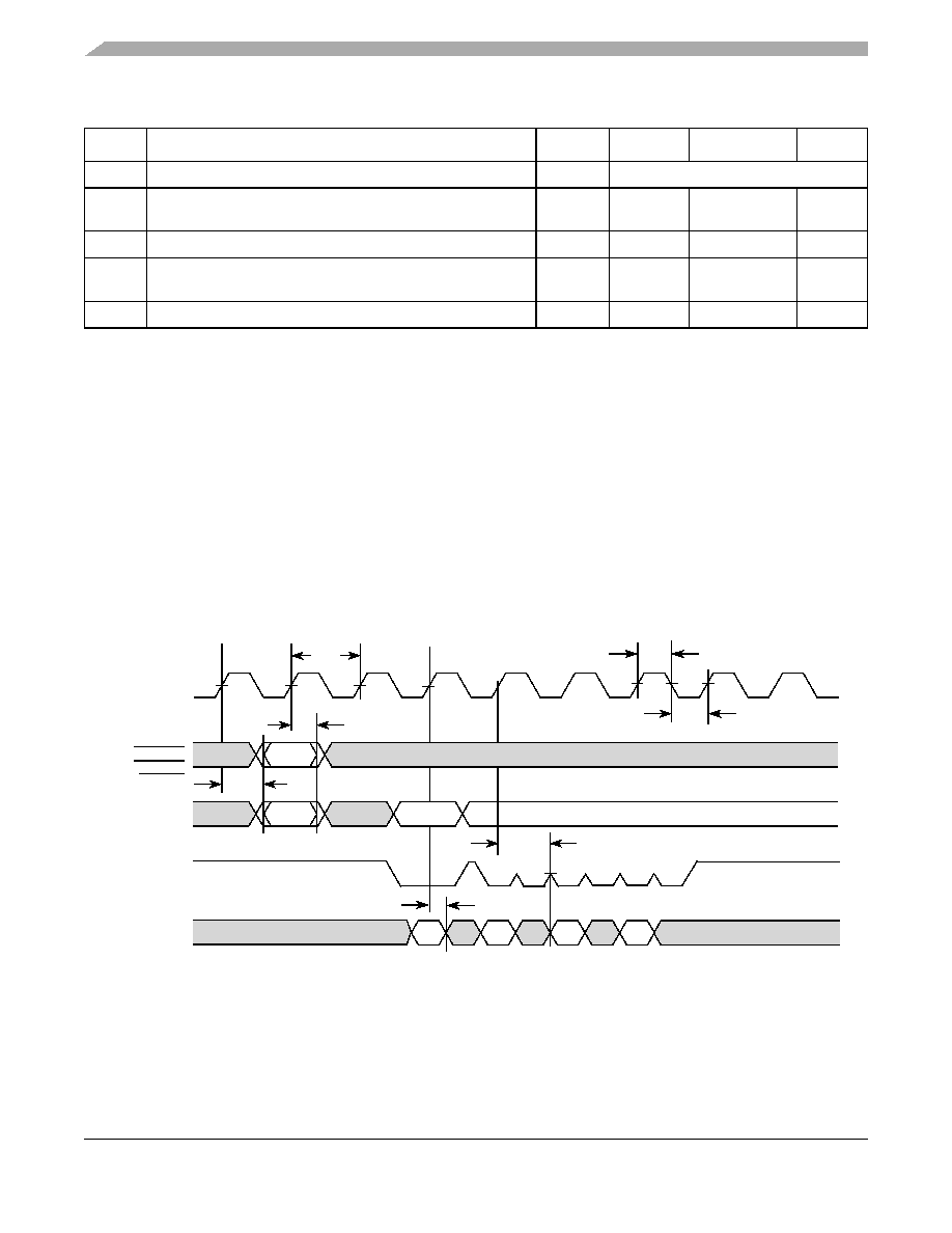
Figure 9. SDR Write Timing
SD9
SD_DQS[3:2] input hold relative to SD_CLK7
tDQISDCH Does not apply. 0.5×SD_CLK fixed width.
SD10
Data (D[31:0]) Input Setup relative to SD_CLK (reference
only)8
tDVSDCH
0.25
×
SD_CLK
—ns
SD11
Data Input Hold relative to SD_CLK (reference only)
tDISDCH
1.0
—
ns
SD12
Data (D[31:0]) and Data Mask(SD_DQM[3:0]) Output Valid
tSDCHDMV
—
0.75
× SD_CLK
+ 0.5
ns
SD13
Data (D[31:0]) and Data Mask (SD_DQM[3:0]) Output Hold
tSDCHDMI
1.5
—
ns
1 The FlexBus and SDRAM clock operates at the same frequency of the internal bus clock. See the PLL chapter of the MCF5373
Reference Manual for more information on setting the SDRAM clock rate.
2 SD_CLK is one SDRAM clock in (ns).
3 Pulse width high plus pulse width low cannot exceed min and max clock period.
4 Pulse width high plus pulse width low cannot exceed min and max clock period.
5 SD_DQS is designed to pulse 0.25 clock before the rising edge of the memory clock. This is a guideline only. Subtle variation
from this guideline is expected. SD_DQS only pulses during a read cycle and one pulse occurs for each data beat.
6 SDR_DQS is designed to pulse 0.25 clock before the rising edge of the memory clock. This spec is a guideline only. Subtle
variation from this guideline is expected. SDR_DQS only pulses during a read cycle and one pulse occurs for each data beat.
7 The SDR_DQS pulse is designed to be 0.5 clock in width. The timing of the rising edge is most important. The falling edge
does not affect the memory controller.
8 Because a read cycle in SDR mode uses the DQS circuit within the device, it is most critical that the data valid window be
centered 1/4 clk after the rising edge of DQS. Ensuring that this happens results in successful SDR reads. The input setup
spec is provided as guidance.
Table 10. SDR Timing Specifications (continued)
Symbol
Characteristic
Symbol
Min
Max
Unit
SD_CLK
SDDM
D[31:0]
A[23:0]
SD_BA[1:0]
CMD
ROW
SD1
SD4
COL
SD5
WD1
WD2
WD3
WD4
SD12
SD11
SD_CSn
SD_RAS
SD_WE
SD_CAS
SD2
SD3
Because
of
an
order
from
the
United
States
International
Trade
Commission,
BGA-packaged
product
lines
and
part
numbers
indicated
here
currently
are
not
available
from
Freescale
for
import
or
sale
in
the
United
States
prior
to
September
2010:
MCF53721CVM240,
MCF5372LCVM240,
MCF5373LCVM240
相关PDF资料 |
PDF描述 |
|---|---|
| MCF5407FT162 | 32-BIT, 162 MHz, RISC PROCESSOR, PQFP208 |
| MCF5407FT220 | 32-BIT, 220 MHz, RISC PROCESSOR, PQFP208 |
| MCF5407CFT162 | 32-BIT, 162 MHz, RISC PROCESSOR, PQFP208 |
| MCF54450VM180 | 32-BIT, 180 MHz, RISC PROCESSOR, BGA256 |
| MCF54454VR266 | 32-BIT, 266 MHz, RISC PROCESSOR, PBGA360 |
相关代理商/技术参数 |
参数描述 |
|---|---|
| MCF5372LCVM240J | 功能描述:32位微控制器 - MCU V3CORE RoHS:否 制造商:Texas Instruments 核心:C28x 处理器系列:TMS320F28x 数据总线宽度:32 bit 最大时钟频率:90 MHz 程序存储器大小:64 KB 数据 RAM 大小:26 KB 片上 ADC:Yes 工作电源电压:2.97 V to 3.63 V 工作温度范围:- 40 C to + 105 C 封装 / 箱体:LQFP-80 安装风格:SMD/SMT |
| MCF5373 | 制造商:FREESCALE 制造商全称:Freescale Semiconductor, Inc 功能描述:ColdFire㈢ Microprocessor |
| MCF5373_08 | 制造商:FREESCALE 制造商全称:Freescale Semiconductor, Inc 功能描述:ColdFire㈢ Microprocessor |
| MCF5373CAB180 | 制造商:FREESCALE 制造商全称:Freescale Semiconductor, Inc 功能描述:Microprocessor Data Sheet |
| MCF5373L | 制造商:FREESCALE 制造商全称:Freescale Semiconductor, Inc 功能描述:ColdFire㈢ Microprocessor |
发布紧急采购,3分钟左右您将得到回复。