- 您现在的位置:买卖IC网 > PDF目录80528 > MCF54453CVR200 (FREESCALE SEMICONDUCTOR INC) 32-BIT, 200 MHz, RISC PROCESSOR, PBGA360 PDF资料下载
参数资料
| 型号: | MCF54453CVR200 |
| 厂商: | FREESCALE SEMICONDUCTOR INC |
| 元件分类: | 微控制器/微处理器 |
| 英文描述: | 32-BIT, 200 MHz, RISC PROCESSOR, PBGA360 |
| 封装: | 23 X 23 MM, ROHS COMPLIANT, TEPBGA-360 |
| 文件页数: | 16/48页 |
| 文件大小: | 945K |
| 代理商: | MCF54453CVR200 |
第1页第2页第3页第4页第5页第6页第7页第8页第9页第10页第11页第12页第13页第14页第15页当前第16页第17页第18页第19页第20页第21页第22页第23页第24页第25页第26页第27页第28页第29页第30页第31页第32页第33页第34页第35页第36页第37页第38页第39页第40页第41页第42页第43页第44页第45页第46页第47页第48页
Electrical Characteristics
MCF5445x ColdFire Microprocessor Data Sheet, Rev. 6
Freescale Semiconductor
23
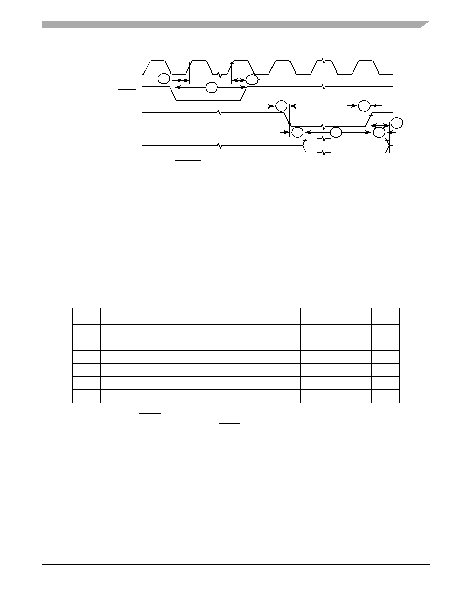
Figure 8. RESET and Configuration Override Timing
5.7
FlexBus Timing Specifications
A multi-function external bus interface called FlexBus is provided with basic functionality to interface to slave-only devices up
to a maximum bus frequency of 66MHz. It can be directly connected to asynchronous or synchronous devices such as external
boot ROMs, flash memories, gate-array logic, or other simple target (slave) devices with little or no additional circuitry. For
asynchronous devices, a simple chip-select based interface can be used.
All processor bus timings are synchronous; input setup/hold and output delay are given in respect to the rising edge of a
reference clock, FB_CLK. The FB_CLK frequency may be the same as the internal system bus frequency or an integer divider
of that frequency.
The following timing numbers indicate when data is latched or driven onto the external bus, relative to the Flexbus output clock
(FB_CLK). All other timing relationships can be derived from these values.
NOTE
The processor drives the data lines during the first clock cycle of the transfer
with the full 32-bit address. This may be ignored by standard connected
devices using non-multiplexed address and data buses. However, some
applications may find this feature beneficial.
The address and data busses are muxed between the FlexBus and PCI
controller. At the end of the read and write bus cycles the address signals are
indeterminate.
Table 12. FlexBus AC Timing Specifications
Num
Characteristic
Min
Max
Unit
Notes
Frequency of Operation
25
66.66
MHz
FB1
Clock Period
15
40
ns
FB2
Output Valid
—
7.0
ns
1
1 Specification is valid for all FB_AD[31:0], FB_BS[3:0], FB_CS[3:0], FB_OE, FB_R/W, FB_TBST,
FB_TSIZ[1:0], and FB_TS.
FB3
Output Hold
1.0
—
ns
1
FB4
Input Setup
3.0
—
ns
2
2 Specification is valid for all FB_AD[31:0] and FB_TA.
FB5
Input Hold
0
—
ns
2
R1
R2
CLKIN
RESET
RSTOUT
R3
R4
R8
R7
R6
R5
Configuration Overrides*:
R4
(BOOTMOD[1:0],
Override pins])
相关PDF资料 |
PDF描述 |
|---|---|
| MC9S12XF128J0MLMR | MICROCONTROLLER, PQFP112 |
| MPC8555ECVTAKD | RISC PROCESSOR, PBGA783 |
| MPC8572CPXAUNB | 32-BIT, 1333 MHz, MICROPROCESSOR, PBGA1023 |
| MPC8572CVTATNB | 32-BIT, 1200 MHz, MICROPROCESSOR, PBGA1023 |
| MPC8572ECVTAVNB | 32-BIT, 1500 MHz, MICROPROCESSOR, PBGA1023 |
相关代理商/技术参数 |
参数描述 |
|---|---|
| MCF54453VR266 | 功能描述:微处理器 - MPU MCF5445X V4M CORE MMU RoHS:否 制造商:Atmel 处理器系列:SAMA5D31 核心:ARM Cortex A5 数据总线宽度:32 bit 最大时钟频率:536 MHz 程序存储器大小:32 KB 数据 RAM 大小:128 KB 接口类型:CAN, Ethernet, LIN, SPI,TWI, UART, USB 工作电源电压:1.8 V to 3.3 V 最大工作温度:+ 85 C 安装风格:SMD/SMT 封装 / 箱体:FBGA-324 |
| MCF54454 | 制造商:FREESCALE 制造商全称:Freescale Semiconductor, Inc 功能描述:ColdFire㈢ Microprocessor |
| MCF54454AVR266 | 制造商:Freescale Semiconductor 功能描述:MCF5445X RISC 32-BIT 266MHZ 1.8V/2.5V/3.3V 360-PIN TEBGA TRA - Trays |
| MCF54454CVR200 | 功能描述:微处理器 - MPU MCF5445X V4M CORE MMU RoHS:否 制造商:Atmel 处理器系列:SAMA5D31 核心:ARM Cortex A5 数据总线宽度:32 bit 最大时钟频率:536 MHz 程序存储器大小:32 KB 数据 RAM 大小:128 KB 接口类型:CAN, Ethernet, LIN, SPI,TWI, UART, USB 工作电源电压:1.8 V to 3.3 V 最大工作温度:+ 85 C 安装风格:SMD/SMT 封装 / 箱体:FBGA-324 |
| MCF54454VR266 | 功能描述:微处理器 - MPU MCF5445X V4M CORE MMU RoHS:否 制造商:Atmel 处理器系列:SAMA5D31 核心:ARM Cortex A5 数据总线宽度:32 bit 最大时钟频率:536 MHz 程序存储器大小:32 KB 数据 RAM 大小:128 KB 接口类型:CAN, Ethernet, LIN, SPI,TWI, UART, USB 工作电源电压:1.8 V to 3.3 V 最大工作温度:+ 85 C 安装风格:SMD/SMT 封装 / 箱体:FBGA-324 |
发布紧急采购,3分钟左右您将得到回复。