- 您现在的位置:买卖IC网 > PDF目录11897 > MCF5474VR266 (Freescale Semiconductor)IC MPU 32BIT COLDF 388-PBGA PDF资料下载
参数资料
| 型号: | MCF5474VR266 |
| 厂商: | Freescale Semiconductor |
| 文件页数: | 11/34页 |
| 文件大小: | 0K |
| 描述: | IC MPU 32BIT COLDF 388-PBGA |
| 标准包装: | 40 |
| 系列: | MCF547x |
| 核心处理器: | Coldfire V4E |
| 芯体尺寸: | 32-位 |
| 速度: | 266MHz |
| 连通性: | EBI/EMI,以太网,I²C,SPI,UART/USART,USB |
| 外围设备: | DMA,PWM,WDT |
| 输入/输出数: | 99 |
| 程序存储器类型: | ROMless |
| RAM 容量: | 32K x 8 |
| 电压 - 电源 (Vcc/Vdd): | 1.43 V ~ 1.58 V |
| 振荡器型: | 外部 |
| 工作温度: | 0°C ~ 70°C |
| 封装/外壳: | 388-BBGA |
| 包装: | 托盘 |
第1页第2页第3页第4页第5页第6页第7页第8页第9页第10页当前第11页第12页第13页第14页第15页第16页第17页第18页第19页第20页第21页第22页第23页第24页第25页第26页第27页第28页第29页第30页第31页第32页第33页第34页
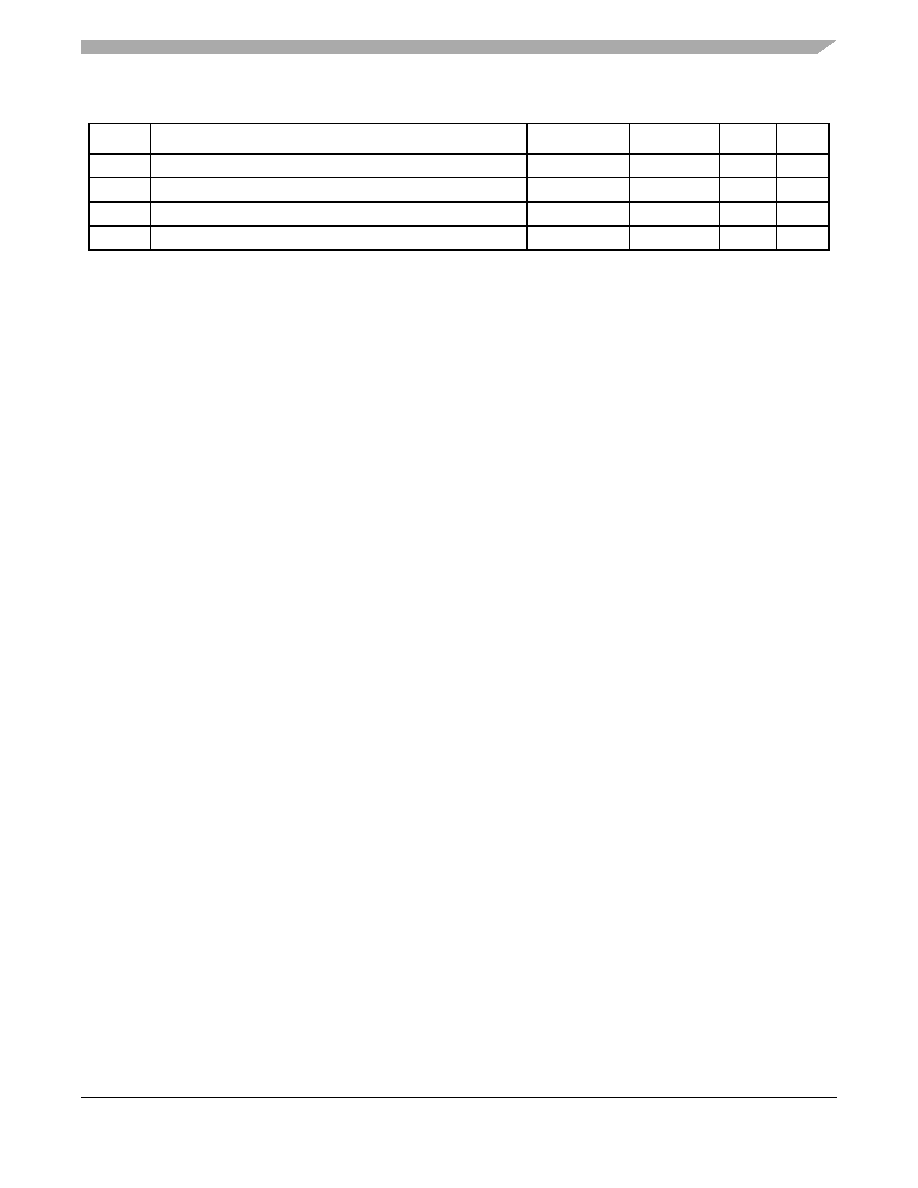
SDRAM Bus
MCF547x ColdFire Microprocessor, Rev. 4
Freescale Semiconductor
19
DD13
DQS input read preamble width (tRPRE)
0.9
1.1
SDCLK
DD14
DQS input read postamble width (tRPST)
0.4
0.6
SDCLK
DD15
DQS output write preamble width (tWPRE)0.25
—
SDCLK
DD16
DQS output write postamble width (tWPST)
0.4
0.6
SDCLK
1
DDR memories typically have a minimum speed specification of 83 MHz. Check memory component specifications to verify.
2 The frequency of operation is 2x or 4x the CLKIN frequency of operation. The MCF547X supports a single external
reference clock (CLKIN). This signal defines the frequency of operation for FlexBus and PCI, but SDRAM clock operates at
the same frequency as the internal bus clock. Please see the reset configuration signals description in the “Signal
Descriptions” chapter within the MCF547x Reference Manual.
3 SDCLK is one memory clock in (ns).
4 Pulse width high plus pulse width low cannot exceed max clock period.
5 Pulse width high plus pulse width low cannot exceed max clock period.
6 Command output valid should be 1/2 the memory bus clock (SDCLK) plus some minor adjustments for process,
temperature, and voltage variations.
7 This specification relates to the required input setup time of today’s DDR memories. SDDATA[31:24] is relative to SDDQS3,
SDDATA[23:16] is relative to SDDQS2, SDDATA[15:8] is relative to SDDQS1, and SDDATA[7:0] is relative SDDQS0.
8 The first data beat is valid before the first rising edge of SDDQS and after the SDDQS write preamble. The remaining data
beats is valid for each subsequent SDDQS edge.
9 This specification relates to the required hold time of today’s DDR memories. SDDATA[31:24] is relative to SDDQS3,
SDDATA[23:16] is relative to SDDQS2, SDDATA[15:8] is relative to SDDQS1, and SDDATA[7:0] is relative SDDQS0.
10 Data input skew is derived from each SDDQS clock edge. It begins with a SDDQS transition and ends when the last data
line becomes valid. This input skew must include DDR memory output skew and system level board skew (due to routing
or other factors).
11 Data input hold is derived from each SDDQS clock edge. It begins with a SDDQS transition and ends when the first data
line becomes invalid.
Table 13. DDR Timing Specifications (continued)
Symbol
Characteristic
Min
Max
Unit
Notes
相关PDF资料 |
PDF描述 |
|---|---|
| V24C15M100BL3 | CONVERTER MOD DC/DC 15V 100W |
| MCF5474ZP266 | IC MPU 32BIT COLDF 388-PBGA |
| MCF5272CVM66J | IC MCU 32BIT 66MHZ 196-MAPBGA |
| MC9S12XDP512MAG | IC MCU 512K FLASH 144-LQFP |
| MC9S12XEP100MAG | IC MCU 16BIT 1M FLASH 144-LQFP |
相关代理商/技术参数 |
参数描述 |
|---|---|
| MCF5474VR266 | 制造商:Freescale Semiconductor 功能描述:Microprocessor IC |
| MCF5474ZP200 | 功能描述:微处理器 - MPU MCF547X V4ECORE MMU FPU RoHS:否 制造商:Atmel 处理器系列:SAMA5D31 核心:ARM Cortex A5 数据总线宽度:32 bit 最大时钟频率:536 MHz 程序存储器大小:32 KB 数据 RAM 大小:128 KB 接口类型:CAN, Ethernet, LIN, SPI,TWI, UART, USB 工作电源电压:1.8 V to 3.3 V 最大工作温度:+ 85 C 安装风格:SMD/SMT 封装 / 箱体:FBGA-324 |
| MCF5474ZP266 | 功能描述:微处理器 - MPU MCF547X V4ECORE MMU FPU RoHS:否 制造商:Atmel 处理器系列:SAMA5D31 核心:ARM Cortex A5 数据总线宽度:32 bit 最大时钟频率:536 MHz 程序存储器大小:32 KB 数据 RAM 大小:128 KB 接口类型:CAN, Ethernet, LIN, SPI,TWI, UART, USB 工作电源电压:1.8 V to 3.3 V 最大工作温度:+ 85 C 安装风格:SMD/SMT 封装 / 箱体:FBGA-324 |
| MCF5475 | 制造商:FREESCALE 制造商全称:Freescale Semiconductor, Inc 功能描述:MCF547x Integrated Microprocessor Electrical Characteristics |
| MCF5475EC | 制造商:FREESCALE 制造商全称:Freescale Semiconductor, Inc 功能描述:MCF547x ColdFire Microprocessor |
发布紧急采购,3分钟左右您将得到回复。