- 您现在的位置:买卖IC网 > PDF目录95921 > MCH3310 (SANYO SEMICONDUCTOR CO LTD) 1500 mA, 30 V, P-CHANNEL, Si, SMALL SIGNAL, MOSFET PDF资料下载
参数资料
| 型号: | MCH3310 |
| 厂商: | SANYO SEMICONDUCTOR CO LTD |
| 元件分类: | 小信号晶体管 |
| 英文描述: | 1500 mA, 30 V, P-CHANNEL, Si, SMALL SIGNAL, MOSFET |
| 封装: | MCPH3, 3 PIN |
| 文件页数: | 1/4页 |
| 文件大小: | 27K |
| 代理商: | MCH3310 |
MCH3310
No.6863-1/4
Features
Low ON-resistance.
Ultrahigh-speed switching.
4V drive.
SANYO Electric Co.,Ltd. Semiconductor Company
TOKYO OFFICE Tokyo Bldg., 1-10, 1 Chome, Ueno, Taito-ku, TOKYO, 110-8534 JAPAN
Ordering number : ENN6863
MCH3310
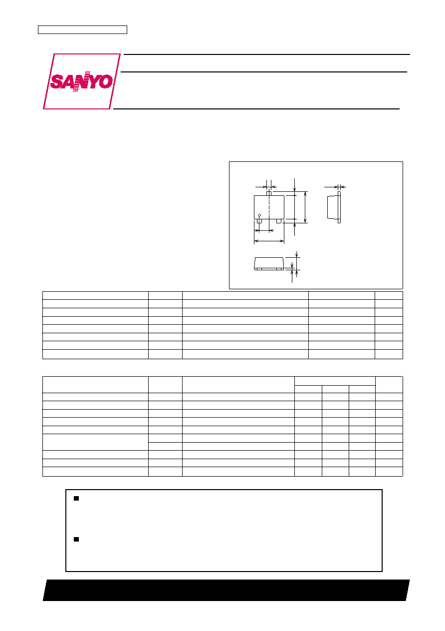
Package Dimensions
unit : mm
2167
[MCH3310]
13001 TS IM TA-3060
Any and all SANYO products described or contained herein do not have specifications that can handle
applications that require extremely high levels of reliability, such as life-support systems, aircraft's
control systems, or other applications whose failure can be reasonably expected to result in serious
physical and/or material damage. Consult with your SANYO representative nearest you before using
any SANYO products described or contained herein in such applications.
SANYO assumes no responsibility for equipment failures that result from using products at values that
exceed, even momentarily, rated values (such as maximum ratings, operating condition ranges, or other
parameters) listed in products specifications of any and all SANYO products described or contained
herein.
P-Channel Silicon MOSFET
Ultrahigh-Speed Switching Applications
1 : Gate
2 : Source
3 : Drain
SANYO : MCPH3
0.25
2.1
1.6
2.0
0.65
0.3
0.85
0.15
12
3
0.15
Specifications
Absolute Maximum Ratings at Ta=25
°C
Parameter
Symbol
Conditions
Ratings
Unit
Drain-to-Source Voltage
VDSS
--30
V
Gate-to-Source Voltage
VGSS
±20
V
Drain Current (DC)
ID
--1.5
A
Drain Current (Pulse)
IDP
PW
≤10s, duty cycle≤1%
--6.0
A
Allowable Power Dissipation
PD
Mounted on a ceramic board (900mm2!0.8mm)
0.9
W
Channel Temperature
Tch
150
°C
Storage Temperature
Tstg
--55 to +150
°C
Electrical Characteristics at Ta=25
°C
Ratings
Parameter
Symbol
Conditions
min
typ
max
Unit
Drain-to-Source Breakdown Voltage
V(BR)DSS
ID=--1mA, VGS=0
--30
V
Zero-Gate Voltage Drain Current
IDSS
VDS=--30V, VGS=0
--1
A
Gate-to-Source Leakage Current
IGSS
VGS=±16V, VDS=0
±10
A
Cutoff Voltage
VGS(off)
VDS=--10V, ID=--1mA
--1.2
--2.6
V
Forward Transfer Admittance
yfs
VDS=--10V, ID=--0.8A
1.0
1.5
S
Static Drain-to-Source On-State Resistance
RDS(on)1
ID=--0.8A, VGS=--10V
210
270
m
RDS(on)2
ID=--0.4A, VGS=--4V
360
500
m
Input Capacitance
Ciss
VDS=--10V, f=1MHz
185
pF
Output Capacitance
Coss
VDS=--10V, f=1MHz
30
pF
Reverse Transfer Capacitance
Crss
VDS=--10V, f=1MHz
20
pF
Marking : JK
Continued on next page.
相关PDF资料 |
PDF描述 |
|---|---|
| MCH3312 | 2000 mA, 30 V, P-CHANNEL, Si, SMALL SIGNAL, MOSFET |
| MCH3314 | 600 mA, 60 V, P-CHANNEL, Si, SMALL SIGNAL, MOSFET |
| MCH3314 | 600 mA, 60 V, P-CHANNEL, Si, SMALL SIGNAL, MOSFET |
| MCH3315 | 1000 mA, 60 V, P-CHANNEL, Si, SMALL SIGNAL, MOSFET |
| MCH3315 | 1000 mA, 60 V, P-CHANNEL, Si, SMALL SIGNAL, MOSFET |
相关代理商/技术参数 |
参数描述 |
|---|---|
| MCH3310-TL-E | 制造商:SANYO 功能描述:Pch 30V 1.5A 0.27 lbogR Tape & Reel 制造商:SANYO Semiconductor Co Ltd 功能描述:MOSFET P CH 30V 1.5A SC-82 |
| MCH3312 | 制造商:SANYO 制造商全称:Sanyo Semicon Device 功能描述:Ultrahigh-Speed Switching Applications |
| MCH3312-TL-E | 制造商:SANYO Semiconductor Co Ltd 功能描述:Cut Tape 制造商:SANYO Semiconductor Co Ltd 功能描述:MOSFET P CH 30V 2A SC-82 |
| MCH3314 | 制造商:SANYO 制造商全称:Sanyo Semicon Device 功能描述:MCH3314 |
| MCH3315 | 制造商:SANYO 制造商全称:Sanyo Semicon Device 功能描述:P-Channel Silicon MOSFET General-Purpose Switching Device Applications |
发布紧急采购,3分钟左右您将得到回复。