- 您现在的位置:买卖IC网 > PDF目录1952 > MCHC11F1CFNE5 (Freescale Semiconductor)MCU 8BIT 1KRAM 512EE 68-PLCC PDF资料下载
参数资料
| 型号: | MCHC11F1CFNE5 |
| 厂商: | Freescale Semiconductor |
| 文件页数: | 4/158页 |
| 文件大小: | 0K |
| 描述: | MCU 8BIT 1KRAM 512EE 68-PLCC |
| 标准包装: | 18 |
| 系列: | HC11 |
| 核心处理器: | HC11 |
| 芯体尺寸: | 8-位 |
| 速度: | 5MHz |
| 连通性: | SCI,SPI |
| 外围设备: | POR,WDT |
| 输入/输出数: | 30 |
| 程序存储器类型: | ROMless |
| EEPROM 大小: | 512 x 8 |
| RAM 容量: | 1K x 8 |
| 电压 - 电源 (Vcc/Vdd): | 4.75 V ~ 5.25 V |
| 数据转换器: | A/D 8x8b |
| 振荡器型: | 内部 |
| 工作温度: | -40°C ~ 85°C |
| 封装/外壳: | 68-LCC(J 形引线) |
| 包装: | 管件 |
第1页第2页第3页当前第4页第5页第6页第7页第8页第9页第10页第11页第12页第13页第14页第15页第16页第17页第18页第19页第20页第21页第22页第23页第24页第25页第26页第27页第28页第29页第30页第31页第32页第33页第34页第35页第36页第37页第38页第39页第40页第41页第42页第43页第44页第45页第46页第47页第48页第49页第50页第51页第52页第53页第54页第55页第56页第57页第58页第59页第60页第61页第62页第63页第64页第65页第66页第67页第68页第69页第70页第71页第72页第73页第74页第75页第76页第77页第78页第79页第80页第81页第82页第83页第84页第85页第86页第87页第88页第89页第90页第91页第92页第93页第94页第95页第96页第97页第98页第99页第100页第101页第102页第103页第104页第105页第106页第107页第108页第109页第110页第111页第112页第113页第114页第115页第116页第117页第118页第119页第120页第121页第122页第123页第124页第125页第126页第127页第128页第129页第130页第131页第132页第133页第134页第135页第136页第137页第138页第139页第140页第141页第142页第143页第144页第145页第146页第147页第148页第149页第150页第151页第152页第153页第154页第155页第156页第157页第158页
SERIAL PERIPHERAL INTERFACE
TECHNICAL DATA
8-3
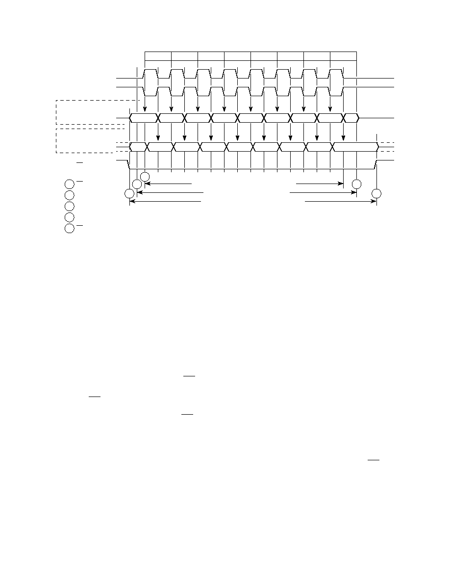
Figure 8-2 SPI Transfer Format
8.2.1 Clock Phase and Polarity Controls
Software can select one of four combinations of serial clock phase and polarity using
two bits in the SPI control register (SPCR). The clock polarity is specified by the CPOL
control bit, which selects an active high or active low clock, and has no significant ef-
fect on the transfer format. The clock phase (CPHA) control bit selects one of two dif-
ferent transfer formats. The clock phase and polarity should be identical for the master
SPI device and the communicating slave device. In some cases, the phase and polar-
ity are changed between transfers to allow a master device to communicate with pe-
ripheral slaves having different requirements.
When CPHA equals zero, the SS line must be negated and reasserted between each
successive serial byte. Also, if the slave writes data to the SPI data register (SPDR)
while SS is low, a write collision error results.
When CPHA equals one, the SS line can remain low between successive transfers.
8.3 SPI Signals
The following paragraphs contain descriptions of the four SPI signals: master in slave
out (MISO), master out slave in (MOSI), serial clock (SCK), and slave select (SS).
Any SPI output line must have its corresponding data direction bit in DDRD register
set. If the DDR bit is clear, that line is disconnected from the SPI logic and becomes a
general-purpose input. All SPI input lines are forced to act as inputs regardless of the
state of the corresponding DDR bits in DDRD register.
2345678
1
SCK (CPOL = 1)
SCK (CPOL = 0)
SCK CYCLE #
SS (TO SLAVE)
654321
LSB
MSB
654321
LSB
SAMPLE INPUT
DATA OUT
SAMPLE INPUT
DATA OUT
(CPHA = 1)
(CPHA = 0)
SLAVE CPHA = 1 TRANSFER IN PROGRESS
MASTER TRANSFER IN PROGRESS
SLAVE CPHA = 0 TRANSFER IN PROGRESS
3
2
1
5
4
SS ASSERTED
MASTER WRITES
FIRST SCK EDGE
SPIF SET
SS NEGATED
1
2
3
4
5
TO SPDR
F
re
e
sc
a
le
S
e
m
ic
o
n
d
u
c
to
r,
I
Freescale Semiconductor, Inc.
For More Information On This Product,
Go to: www.freescale.com
n
c
..
.
相关PDF资料 |
PDF描述 |
|---|---|
| MCHC908JW32FC | IC MCU 32K FLASH 8MHZ 48-QFN |
| MCHC908MR8MFAE | IC MCU 8K FLASH 8MHZ PWM 32-LQFP |
| MCHRC705J1ACDWE | MCU 8BIT 64B RAM 20-SOIC |
| MCIMX233CAG4C | MPU 32BIT I.MX233 IND 128LQFP |
| MCIMX233DJM4B | MPU 32BIT I.MX233 169MAPBGA |
相关代理商/技术参数 |
参数描述 |
|---|---|
| MCHC11F1MFNE4 | 制造商:Freescale Semiconductor 功能描述:8-BIT MCU,1KRAM,512EE,A/ - Rail/Tube |
| MCHC11F1VFNE3 | 功能描述:8位微控制器 -MCU 8B MCU 1KRAM 512EE RoHS:否 制造商:Silicon Labs 核心:8051 处理器系列:C8051F39x 数据总线宽度:8 bit 最大时钟频率:50 MHz 程序存储器大小:16 KB 数据 RAM 大小:1 KB 片上 ADC:Yes 工作电源电压:1.8 V to 3.6 V 工作温度范围:- 40 C to + 105 C 封装 / 箱体:QFN-20 安装风格:SMD/SMT |
| MCHC11KS1CFNE4 | 功能描述:8位微控制器 -MCU 68HC11KS4 RoHS:否 制造商:Silicon Labs 核心:8051 处理器系列:C8051F39x 数据总线宽度:8 bit 最大时钟频率:50 MHz 程序存储器大小:16 KB 数据 RAM 大小:1 KB 片上 ADC:Yes 工作电源电压:1.8 V to 3.6 V 工作温度范围:- 40 C to + 105 C 封装 / 箱体:QFN-20 安装风格:SMD/SMT |
| MCHC175AFR1 | 制造商:Rochester Electronics LLC 功能描述:- Bulk |
| MCHC40-330K-RC | 制造商:ALLIED 制造商全称:Allied Components International 功能描述:Molded Chip Inductor High Current |
发布紧急采购,3分钟左右您将得到回复。